


TMS320F2809, TMS320F2808, TMS320F2806
TMS320F2802, TMS320F2801, TMS320C2802
TMS320C2801, TMS320F28016, TMS320F28015
www.ti.com
SPRS230L–OCTOBER 2003–REVISED DECEMBER 2009
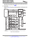
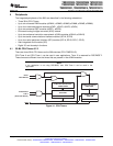
3.6.1.2 PLL-Based Clock Module
The 280x devices have an on-chip, PLL-based clock module. This module provides all the necessary
clocking signals for the device, as well as control for low-power mode entry. The PLL has a 4-bit ratio
control PLLCR[DIV] to select different CPU clock rates. The watchdog module should be disabled before
writing to the PLLCR register. It can be re-enabled (if need be) after the PLL module has stabilized, which
takes 131072 OSCCLK cycles.
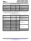
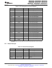
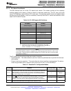
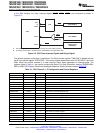
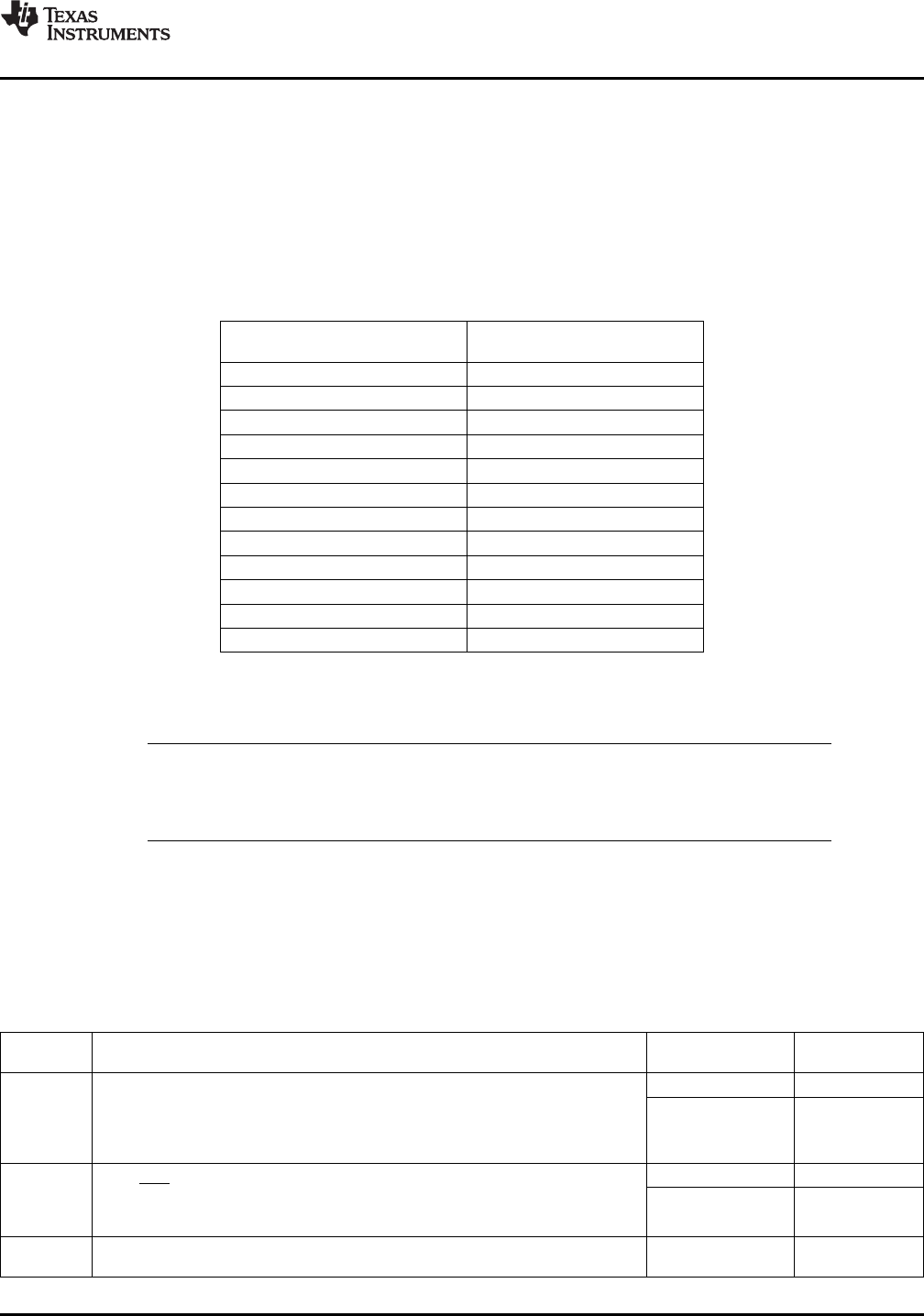
Table 3-16. PLLCR Register Bit Definitions
SYSCLKOUT
PLLCR[DIV]
(1)
(CLKIN)
(2)
0000 (PLL bypass) OSCCLK/n
0001 (OSCCLK*1)/n
0010 (OSCCLK*2)/n
0011 (OSCCLK*3)/n
0100 (OSCCLK*4)/n
0101 (OSCCLK*5)/n
0110 (OSCCLK*6)/n
0111 (OSCCLK*7)/n
1000 (OSCCLK*8)/n
1001 (OSCCLK*9)/n
1010 (OSCCLK*10)/n
1011–1111 Reserved
(1) This register is EALLOW protected.
(2) CLKIN is the input clock to the CPU. SYSCLKOUT is the output
clock from the CPU. The frequency of SYSCLKOUT is the same as
CLKIN. If CLKINDIV = 0, n = 2; if CLKINDIV = 1, n = 1.
NOTE
PLLSTS[CLKINDIV] enables or bypasses the divide-by-two block before the clock is fed
to the core. This bit must be 0 before writing to the PLLCR and must only be set after
PLLSTS[PLLLOCKS] = 1.
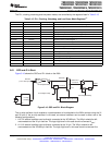
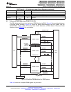
The PLL-based clock module provides two modes of operation:
• Crystal-operation - This mode allows the use of an external crystal/resonator to provide the time base
to the device.
• External clock source operation - This mode allows the internal oscillator to be bypassed. The device
clocks are generated from an external clock source input on the X1 or the XCLKIN pin.
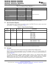
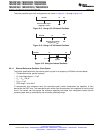
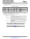
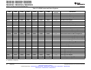
Table 3-17. Possible PLL Configuration Modes
SYSCLKOUT
PLL MODE REMARKS PLLSTS[CLKINDIV]
(CLKIN)
Invoked by the user setting the PLLOFF bit in the PLLSTS register. The PLL block 0 OSCCLK/2
is disabled in this mode. This can be useful to reduce system noise and for low
PLL Off power operation. The PLLCR register must first be set to 0x0000 (PLL Bypass)
1 OSCCLK
before entering this mode. The CPU clock (CLKIN) is derived directly from the
input clock on either X1/X2, X1 or XCLKIN.
PLL Bypass is the default PLL configuration upon power-up or after an external 0 OSCCLK/2
reset (XRS). This mode is selected when the PLLCR register is set to 0x0000 or
PLL Bypass
while the PLL locks to a new frequency after the PLLCR register has been
1 OSCCLK
modified. In this mode, the PLL itself is bypassed but the PLL is not turned off.
Achieved by writing a non-zero value n into the PLLCR register. Upon writing to the
PLL Enable 0 OSCCLK*n/2
PLLCR the device will switch to PLL Bypass mode until the PLL locks.
Copyright © 2003–2009, Texas Instruments Incorporated Functional Overview 49
Submit Documentation Feedback
Product Folder Link(s): TMS320F2809 TMS320F2808 TMS320F2806 TMS320F2802 TMS320F2801 TMS320C2802
TMS320C2801 TMS320F28016 TMS320F28015