


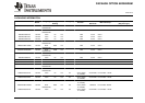
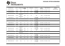
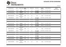

TMS320F2809, TMS320F2808, TMS320F2806
TMS320F2802, TMS320F2801, TMS320C2802
TMS320C2801, TMS320F28016, TMS320F28015
www.ti.com
SPRS230L–OCTOBER 2003–REVISED DECEMBER 2009
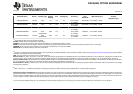
7 Migrating From F280x Devices to C280x Devices
7.1 Migration Issues
The migration issues to be considered while migrating from the F280x devices to C280x devices are as
follows:
• The 1K OTP memory available in F280x devices has been replaced by 1K ROM C280x devices.
• Current consumption differs for F280x and C280x devices for all four possible modes. See the
appropriate electrical section for exact numbers.
• The V
DD3VFL
pin is the 3.3-V Flash core power pin in F280x devices but is a V
DDIO
pin in C280x
devices.
• F280x and C280x devices are pin-compatible and code-compatible; however, they are electrically
different with different EMI/ESD profiles. Before ramping production with C280x devices, evaluate
performance of the hardware design with both devices.
• Addresses 0x3D 7BFC through 0x3D 7BFF in the OTP and addresses 0x3F 7FF0 through 0x3F 7FF5
in the main ROM array are reserved for ROM part-specific information and are not available for user
applications.
• The paged and random wait-state specifications for the Flash and ROM parts are different. While
migrating from Flash to ROM parts, the same wait-state values must be used for best-performance
compatibility (for example, in applications that use software delay loops or where precise interrupt
latencies are critical).
• The analog input switch resistance is smaller in C280x devices compared to F280x devices. While
migrating from a Flash to a ROM device care should be taken to design the analog input circuits to
meet the application performance required by the sampling network.
• The PART-ID register value is different for Flash and ROM parts.
• From a silicon functionality/errata standpoint, rev A ROM devices are equivalent to rev C flash devices.
See the errata applicable to 280x devices for details.
• As part of the ROM code generation process, all unused memory locations in the customer application
are automatically filled with 0xFFFF. Unused locations should not be manually filled with any other
data.
For errata applicable to 280x devices, see the TMS320F280x, TMS320C280x, and TMS320F2801x DSC
Silicon Errata (literature number SPRZ171).
Copyright © 2003–2009, Texas Instruments Incorporated Migrating From F280x Devices to C280x Devices 133
Submit Documentation Feedback
Product Folder Link(s): TMS320F2809 TMS320F2808 TMS320F2806 TMS320F2802 TMS320F2801 TMS320C2802
TMS320C2801 TMS320F28016 TMS320F28015