


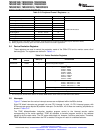
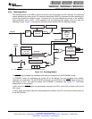
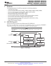
X1
XCLKIN
(3.3-V clock input)
On chip
oscillator
X2
xor
PLLSTS[OSCOFF]
OSCCLK
PLL
VCOCLK
4-bit PLL Select (PLLCR)
OSCCLK or
VCOCLK
CLKIN
OSCCLK
0
PLLSTS[PLLOFF]
n
n ≠ 0
/2
PLLSTS[CLKINDIV]
TMS320F2809, TMS320F2808, TMS320F2806
TMS320F2802, TMS320F2801, TMS320C2802
TMS320C2801, TMS320F28016, TMS320F28015
www.ti.com
SPRS230L–OCTOBER 2003–REVISED DECEMBER 2009
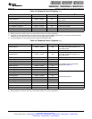
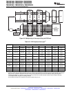
The PLL, clocking, watchdog and low-power modes, are controlled by the registers listed in Table 3-15.
Table 3-15. PLL, Clocking, Watchdog, and Low-Power Mode Registers
(1)
NAME ADDRESS SIZE (x16) DESCRIPTION
XCLK 0x7010 1 XCLKOUT Pin Control, X1 and XCLKIN Status Register
PLLSTS 0x7011 1 PLL Status Register
Reserved 0x7012 – 0x7019 8 Reserved
HISPCP 0x701A 1 High-Speed Peripheral Clock Prescaler Register (for HSPCLK)
LOSPCP 0x701B 1 Low-Speed Peripheral Clock Prescaler Register (for LSPCLK)
PCLKCR0 0x701C 1 Peripheral Clock Control Register 0
PCLKCR1 0x701D 1 Peripheral Clock Control Register 1
LPMCR0 0x701E 1 Low Power Mode Control Register 0
Reserved 0x701F – 0x7020 1 Reserved
PLLCR 0x7021 1 PLL Control Register
SCSR 0x7022 1 System Control and Status Register
WDCNTR 0x7023 1 Watchdog Counter Register
Reserved 0x7024 1 Reserved
WDKEY 0x7025 1 Watchdog Reset Key Register
Reserved 0x7026 – 0x7028 3 Reserved
WDCR 0x7029 1 Watchdog Control Register
Reserved 0x702A – 0x702F 6 Reserved
(1) All of the registers in this table are EALLOW protected.
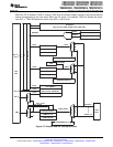
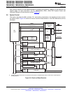
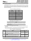
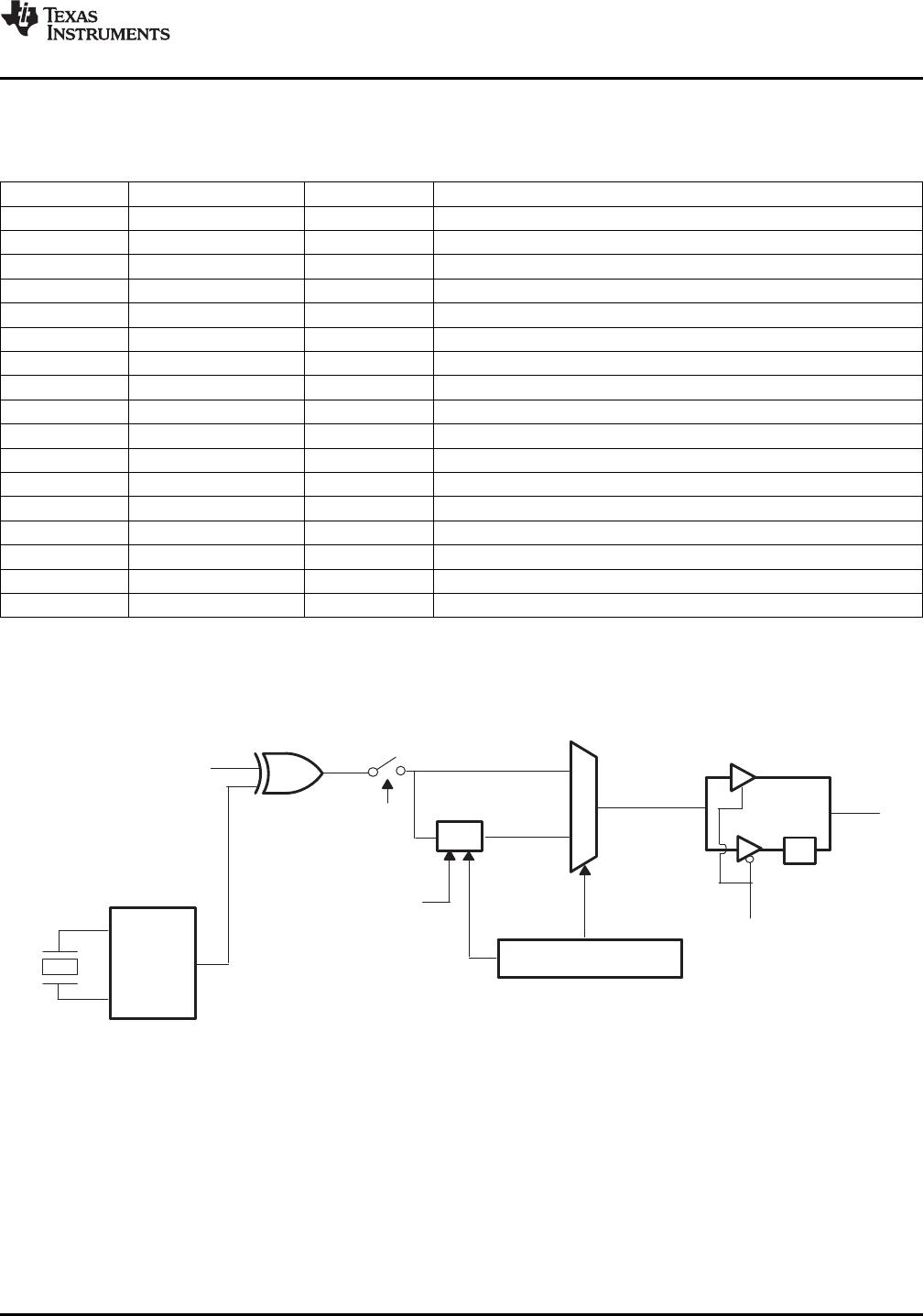
3.6.1 OSC and PLL Block
Figure 3-10 shows the OSC and PLL block on the 280x.
Figure 3-10. OSC and PLL Block Diagram
The on-chip oscillator circuit enables a crystal/resonator to be attached to the 280x devices using the X1
and X2 pins. If the on-chip oscillator is not used, an external oscillator can be used in either one of the
following configurations:
1. A 3.3-V external oscillator can be directly connected to the XCLKIN pin. The X2 pin should be left
unconnected and the X1 pin tied low. The logic-high level in this case should not exceed V
DDIO
.
2. A 1.8-V external oscillator can be directly connected to the X1 pin. The X2 pin should be left
unconnected and the XCLKIN pin tied low. The logic-high level in this case should not exceed V
DD
.
Copyright © 2003–2009, Texas Instruments Incorporated Functional Overview 47
Submit Documentation Feedback
Product Folder Link(s): TMS320F2809 TMS320F2808 TMS320F2806 TMS320F2802 TMS320F2801 TMS320C2802
TMS320C2801 TMS320F28016 TMS320F28015