


TMS320F2809, TMS320F2808, TMS320F2806
TMS320F2802, TMS320F2801, TMS320C2802
TMS320C2801, TMS320F28016, TMS320F28015
www.ti.com
SPRS230L–OCTOBER 2003–REVISED DECEMBER 2009
List of Tables
2-1 Hardware Features (100-MHz Devices)....................................................................................... 12
2-2 Hardware Features (60-MHz Devices) ........................................................................................ 13
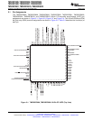
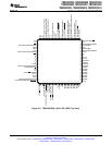
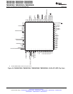
2-3 Signal Descriptions............................................................................................................... 19
3-1 Addresses of Flash Sectors in F2809 ......................................................................................... 31
3-2 Addresses of Flash Sectors in F2808 ......................................................................................... 31
3-3 Addresses of Flash Sectors in F2806, F2802 ................................................................................ 31
3-4 Addresses of Flash Sectors in F2801, F28015, F28016.................................................................... 32
3-5 Impact of Using the Code Security Module................................................................................... 32
3-6 Wait-states ........................................................................................................................ 33
3-7 Boot Mode Selection............................................................................................................. 36
3-8 Peripheral Frame 0 Registers .................................................................................................. 41
3-9 Peripheral Frame 1 Registers .................................................................................................. 41
3-10 Peripheral Frame 2 Registers .................................................................................................. 42
3-11 Device Emulation Registers..................................................................................................... 42
3-12 PIE Peripheral Interrupts ....................................................................................................... 44
3-13 PIE Configuration and Control Registers...................................................................................... 45
3-14 External Interrupt Registers..................................................................................................... 45
3-15 PLL, Clocking, Watchdog, and Low-Power Mode Registers .............................................................. 47
3-16 PLLCR Register Bit Definitions................................................................................................. 49
3-17 Possible PLL Configuration Modes ............................................................................................ 49
3-18 Low-Power Modes ............................................................................................................... 52
4-1 CPU-Timers 0, 1, 2 Configuration and Control Registers................................................................... 54
4-2 ePWM Control and Status Registers .......................................................................................... 56
4-3 eCAP Control and Status Registers ........................................................................................... 60
4-4 eQEP Control and Status Registers ........................................................................................... 62
4-5 ADC Registers ................................................................................................................... 67
4-6 3.3-V eCAN Transceivers ...................................................................................................... 69
4-7 CAN Register Map .............................................................................................................. 72
4-8 SCI-A Registers .................................................................................................................. 74
4-9 SCI-B Registers .................................................................................................................. 74
4-10 SPI-A Registers................................................................................................................... 77
4-11 SPI-B Registers................................................................................................................... 77
4-12 SPI-C Registers .................................................................................................................. 78
4-13 SPI-D Registers .................................................................................................................. 78
4-14 I2C-A Registers................................................................................................................... 81
4-15 GPIO Registers .................................................................................................................. 83
4-16 F2808 GPIO MUX Table ........................................................................................................ 84
5-1 TMS320x280x, 2801x Peripheral Selection Guide .......................................................................... 88
6-1 TMS320F2809, TMS320F2808 Current Consumption by Power-Supply Pins at 100-MHz SYSCLKOUT........... 95
6-2 TMS320F2806 Current Consumption by Power-Supply Pins at 100-MHz SYSCLKOUT ............................. 96
6-3 TMS320F2802, TMS320F2801 Current Consumption by Power-Supply Pins at 100-MHz SYSCLKOUT........... 97
6-4 TMS320C2802, TMS320C2801 Current Consumption by Power-Supply Pins at 100-MHz SYSCLKOUT .......... 98
6-5 Typical Current Consumption by Various Peripherals (at 100 MHz) ..................................................... 99
6-6 TMS320x280x Clock Table and Nomenclature (100-MHz Devices)..................................................... 104
6-7 TMS320x280x/2801x Clock Table and Nomenclature (60-MHz Devices) .............................................. 104
6-8 Input Clock Frequency ......................................................................................................... 105
Copyright © 2003–2009, Texas Instruments Incorporated List of Tables 7