


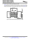
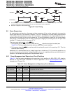
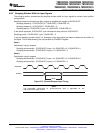
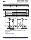
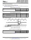
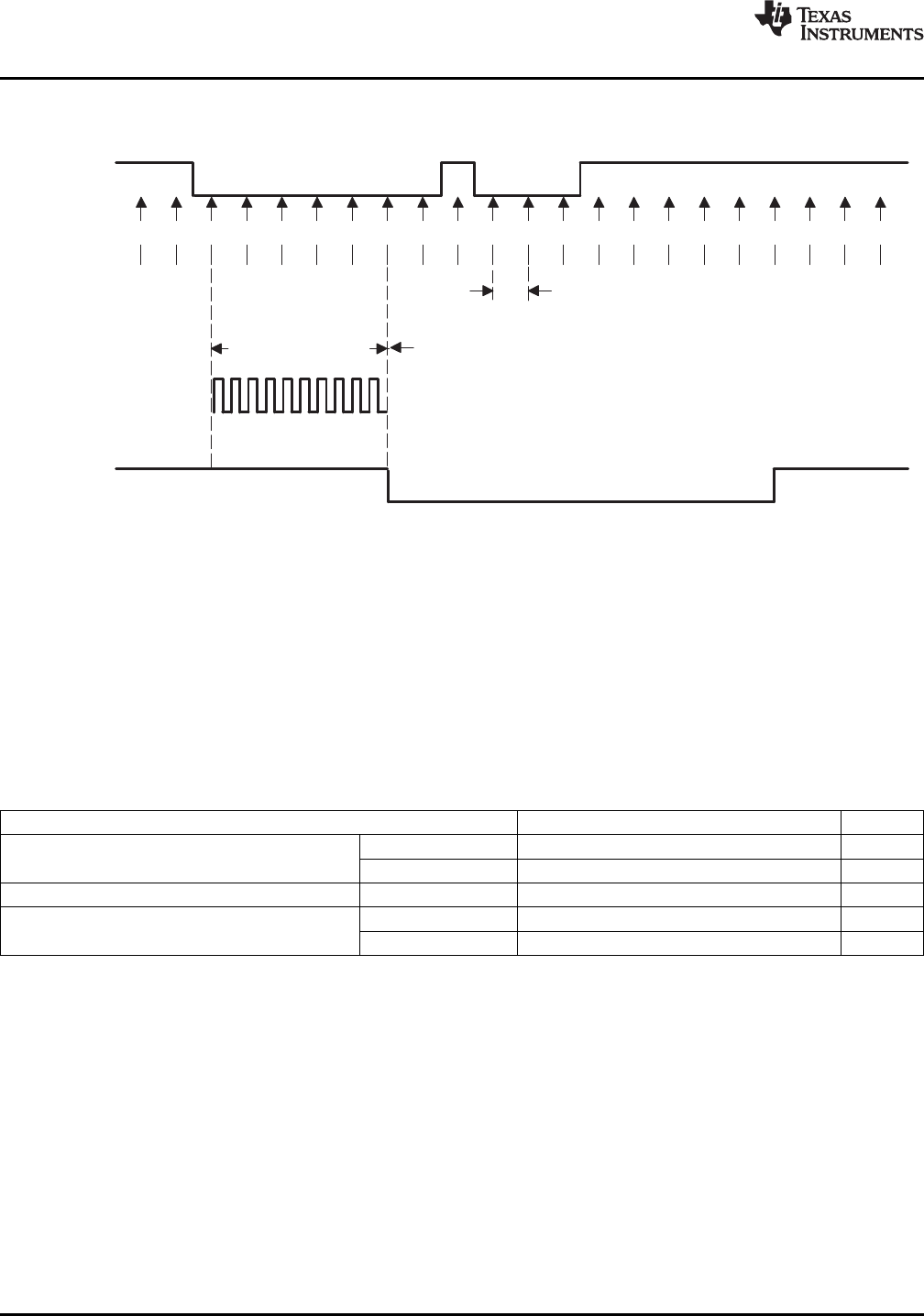
GPIO Signal
1
Sampling Window
Output From
Qualifier
1 1 1 1 1 1 1 1 1 1 10 0 0 0 0 0 0 0 0 0
SYSCLKOUT
QUALPRD = 1
(SYSCLKOUT/2)
(SYSCLKOUT cycle * 2 * QUALPRD) * 5
(C)
)
(A)
GPxQSELn = 1,0 (6 samples)
Sampling Period determined
by GPxCTRL[QUALPRD]
(B)
(D)
t
w(SP)
t
w(IQSW)
TMS320F2809, TMS320F2808, TMS320F2806
TMS320F2802, TMS320F2801, TMS320C2802
TMS320C2801, TMS320F28016, TMS320F28015
SPRS230L–OCTOBER 2003–REVISED DECEMBER 2009
www.ti.com
6.9.2 GPIO - Input Timing
A. This glitch will be ignored by the input qualifier. The QUALPRD bit field specifies the qualification sampling period. It
can vary from 00 to 0xFF. If QUALPRD = 00, then the sampling period is 1 SYSCLKOUT cycle. For any other value
"n", the qualification sampling period in 2n SYSCLKOUT cycles (i.e., at every 2n SYSCLKOUT cycles, the GPIO pin
will be sampled).
B. The qualification period selected via the GPxCTRL register applies to groups of 8 GPIO pins.
C. The qualification block can take either three or six samples. The GPxQSELn Register selects which sample mode is
used.
D. In the example shown, for the qualifier to detect the change, the input should be stable for 10 SYSCLKOUT cycles or
greater. In other words, the inputs should be stable for (5 x QUALPRD x 2) SYSCLKOUT cycles. This would ensure
5 sampling periods for detection to occur. Since external signals are driven asynchronously, an 13-SYSCLKOUT-wide
pulse ensures reliable recognition.
Figure 6-12. Sampling Mode
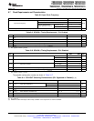
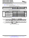
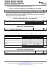
Table 6-15. General-Purpose Input Timing Requirements
MIN MAX UNIT
QUALPRD = 0 1t
c(SCO)
cycles
t
w(SP)
Sampling period
QUALPRD ≠ 0 2t
c(SCO)
* QUALPRD cycles
t
w(IQSW)
Input qualifier sampling window t
w(SP)
* (n
(1)
– 1) cycles
Synchronous mode 2t
c(SCO)
cycles
t
w(GPI)
(2)
Pulse duration, GPIO low/high
With input qualifier t
w(IQSW)
+ t
w(SP)
+ 1t
c(SCO)
cycles
(1) "n" represents the number of qualification samples as defined by GPxQSELn register.
(2) For t
w(GPI)
, pulse width is measured from V
IL
to V
IL
for an active low signal and V
IH
to V
IH
for an active high signal.
110 Electrical Specifications Copyright © 2003–2009, Texas Instruments Incorporated
Submit Documentation Feedback
Product Folder Link(s): TMS320F2809 TMS320F2808 TMS320F2806 TMS320F2802 TMS320F2801 TMS320C2802
TMS320C2801 TMS320F28016 TMS320F28015