


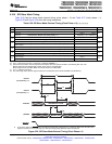
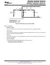
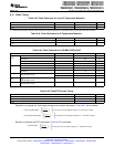
+
ƪ
ǒ
t
a(fp)
t
c(SCO)
Ǔ *1
ƫ
(round up to the next highest integer) or 0, whichever is larger
(round up to the next highest integer) or 1, whichever is larger
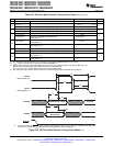
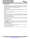
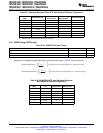
+
ƪ
ǒ
t
a(fr)
t
c(SCO)
Ǔ *1
ƫ
Flash Page Wait-State
Flash Random Wait-State
(round up to the next highest integer) or 1, whichever is larger
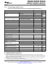
+
ƪ
ǒ
t
a(OTP)
t
c(SCO)
Ǔ *1
ƫ
OTP Wait-State
TMS320F2809, TMS320F2808, TMS320F2806
TMS320F2802, TMS320F2801, TMS320C2802
TMS320C2801, TMS320F28016, TMS320F28015
www.ti.com
SPRS230L–OCTOBER 2003–REVISED DECEMBER 2009
6.12 Flash Timing
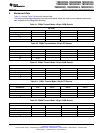
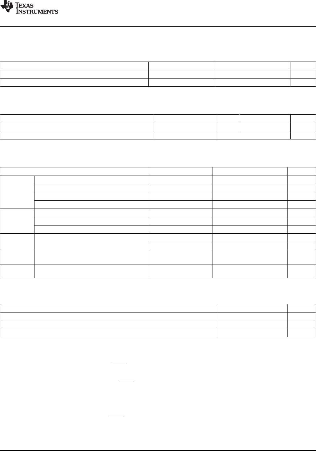
Table 6-43. Flash Endurance for A and S Temperature Material
(1)
MIN TYP MAX UNIT
N
f
Flash endurance for the array (write/erase cycles) 0°C to 85°C (ambient) 20000 50000 cycles
N
OTP
OTP endurance for the array (write cycles) 0°C to 85°C (ambient) 1 write
(1) Write/erase operations outside of the temperature ranges indicated are not specified and may affect the endurance numbers.
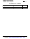
Table 6-44. Flash Endurance for Q Temperature Material
(1)
MIN TYP MAX UNIT
N
f
Flash endurance for the array (write/erase cycles) –40°C to 125°C (ambient) 20000 50000 cycles
N
OTP
OTP endurance for the array (write cycles) –40°C to 125°C (ambient) 1 write
(1) Write/erase operations outside of the temperature ranges indicated are not specified and may affect the endurance numbers.
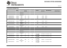
Table 6-45. Flash Parameters at 100-MHz SYSCLKOUT
PARAMETER
(1)
TEST CONDITIONS MIN TYP MAX UNIT
Program 16-Bit Word 50 μs
Time
16K Sector 500 ms
8K Sector 250 ms
4K Sector 125 ms
Erase Time 16K Sector 10 S
8K Sector 10 S
4K Sector 10 S
I
DD3VFLP
V
DD3VFL
current consumption during the Erase 75 mA
Erase/Program cycle
Program 35 mA
I
DDP
V
DD
current consumption during 140 mA
Erase/Program cycle
I
DDIOP
V
DDIO
current consumption during 20 mA
Erase/Program cycle
(1) Typical parameters as seen at room temperature including function call overhead, with all peripherals off.
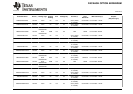
Table 6-46. Flash/OTP Access Timing
PARAMETER MIN TYP MAX UNIT
t
a(fp)
Paged flash access time 36 ns
t
a(fr)
Random flash access time 36 ns
t
a(OTP)
OTP access time 60 ns
Equations to compute the Flash page wait-state and random wait-state in Table 6-47 are as follows:
Equation to compute the OTP wait-state in Table 6-47 is as follows:
Copyright © 2003–2009, Texas Instruments Incorporated Electrical Specifications 131
Submit Documentation Feedback
Product Folder Link(s): TMS320F2809 TMS320F2808 TMS320F2806 TMS320F2802 TMS320F2801 TMS320C2802
TMS320C2801 TMS320F28016 TMS320F28015