


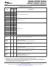
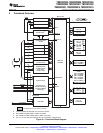
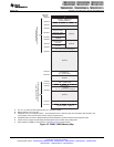
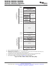
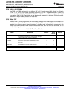
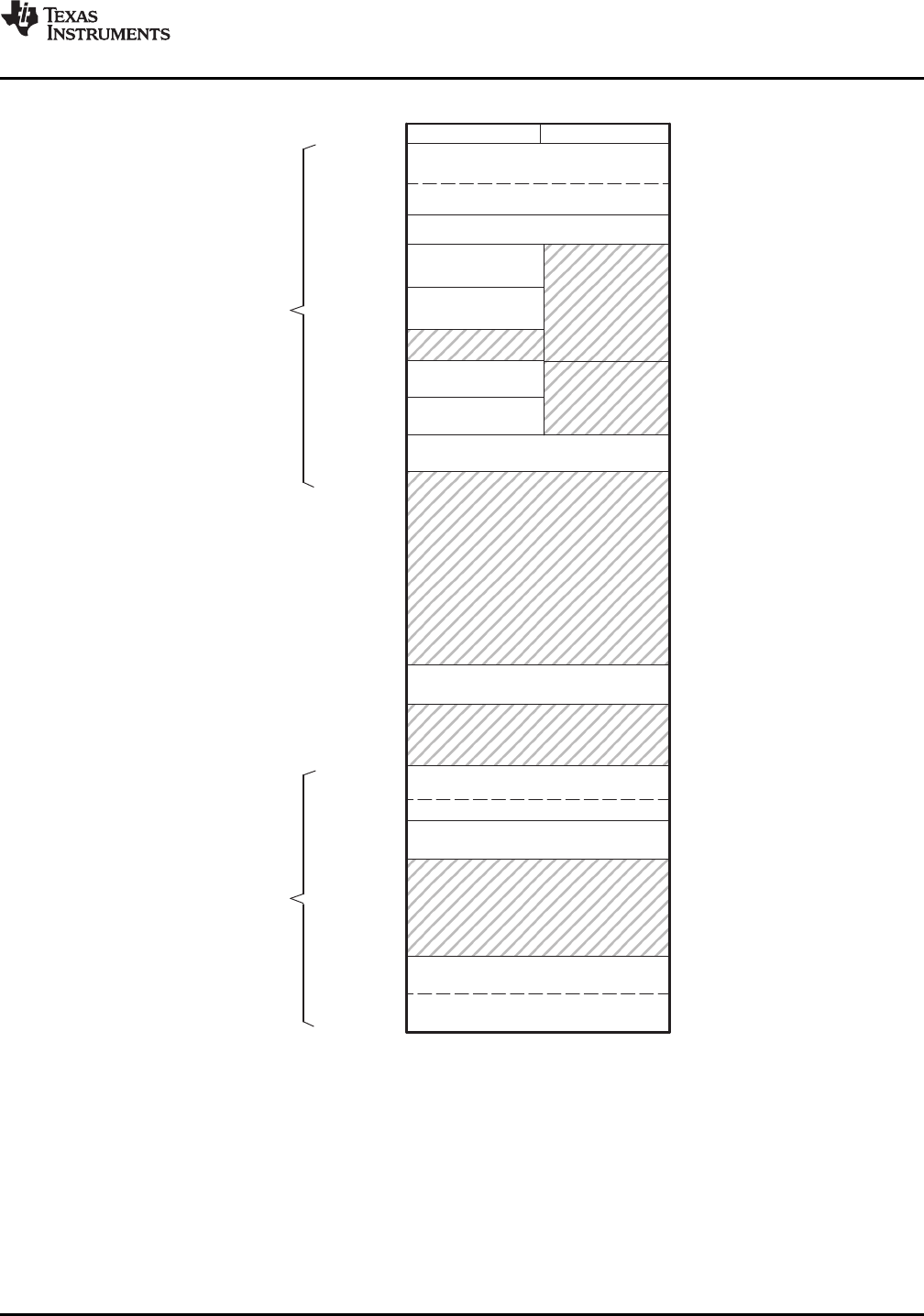
0x00 0000
Block Start
Address
0x00 0400
0x00 0800
0x00 0D00
0x00 6000
0x00 7000
0x00 8000
0x00 9000
0x3D 7800
0x3F 0000
0x3F 7FF8
0x3F 8000
0x3F 9000
0x3F F000
0x3F FFC0
OTP (F2802 Only)
(A)
(1K y 16, Secure Zone)
FLASH (F2802) or ROM (C2802)
(32K y 16, Secure Zone)
L0 (0-wait)
(4K y 16, Secure Zone, Dual-Mapped)
Boot ROM (4K y 16)
128-bit Password
Data Space Prog Space
0x3D 7C00
Vectors (32 y 32)
(enabled if VMAP = 1, ENPIE = 0)
Low 64K [0000−FFFF]
(24x/240x equivalent data space)
High 64K [3F0000 −3FFFF]
(24x/240x equivalent program space)
M0 SARAM (1K y 16)
M1 SARAM (1K y 16)
Peripheral Frame 0
Peripheral Frame 1
(protected)
Peripheral Frame 2
(protected)
L0 SARAM (0-wait)
(4K y 16, Secure Zone, Dual-Mapped)
PIE Vector − RAM
(256 x 16)
(Enabled if ENPIE = 1)
0x00 0E00
Reserved
Reserved
Reserved
Reserved
Reserved
Reserved
0x00 0040
M0 Vector − RAM (32 x 32)
(Enabled if VMAP = 0)
TMS320F2809, TMS320F2808, TMS320F2806
TMS320F2802, TMS320F2801, TMS320C2802
TMS320C2801, TMS320F28016, TMS320F28015
www.ti.com
SPRS230L–OCTOBER 2003–REVISED DECEMBER 2009
A. The 1K x 16 OTP has been replaced with 1K x 16 ROM in C2802.
B. Memory blocks are not to scale.
C. Peripheral Frame 0, Peripheral Frame 1, and Peripheral Frame 2 memory maps are restricted to data memory only.
User program cannot access these memory maps in program space.
D. Protected means the order of Write followed by Read operations is preserved rather than the pipeline order.
E. Certain memory ranges are EALLOW protected against spurious writes after configuration.
F. Some locations in ROM are reserved for TI. See Table 3-5 for more information.
Figure 3-5. F2802, C2802 Memory Map
Copyright © 2003–2009, Texas Instruments Incorporated Functional Overview 29
Submit Documentation Feedback
Product Folder Link(s): TMS320F2809 TMS320F2808 TMS320F2806 TMS320F2802 TMS320F2801 TMS320C2802
TMS320C2801 TMS320F28016 TMS320F28015