


OSCCLK
SYSCLKOUT
Write to PLLCR
OSCCLK * 2
(Current CPU
Frequency)
OSCCLK/2
(CPU Frequency While PLL is Stabilizing
With the Desired Frequency. This Period
(PLL Lock-up Time, t
p
) is
131072 OSCCLK Cycles Long.)
OSCCLK * 4
(Changed CPU Frequency)
GPIO
t
r(GPO)
t
f(GPO)
TMS320F2809, TMS320F2808, TMS320F2806
TMS320F2802, TMS320F2801, TMS320C2802
TMS320C2801, TMS320F28016, TMS320F28015
www.ti.com
SPRS230L–OCTOBER 2003–REVISED DECEMBER 2009
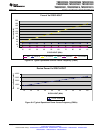
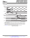
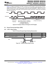
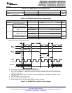
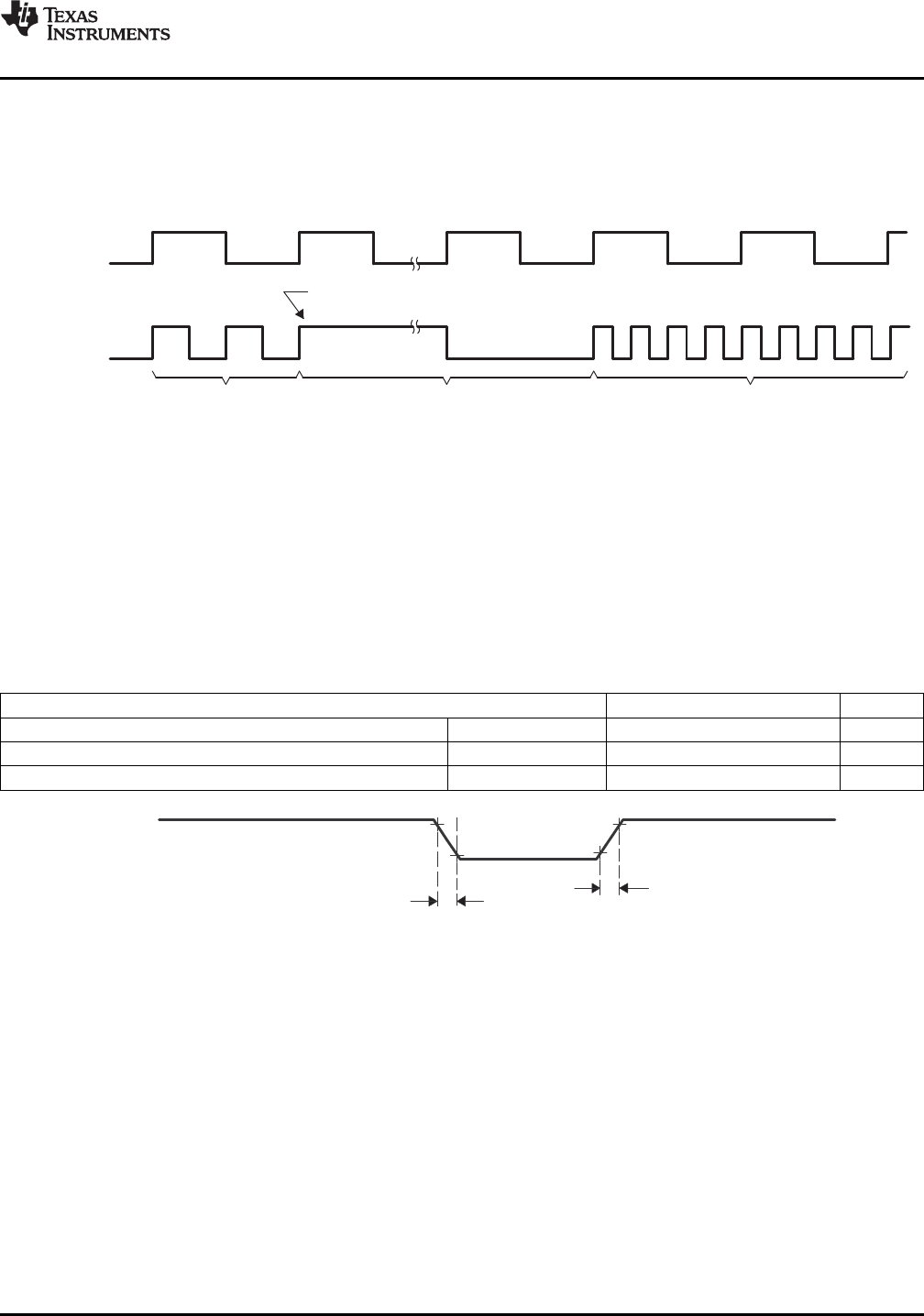
Figure 6-10 shows an example for the effect of writing into PLLCR register. In the first phase, PLLCR =
0x0004 and SYSCLKOUT = OSCCLK x 2. The PLLCR is then written with 0x0008. Right after the PLLCR
register is written, the PLL lock-up phase begins. During this phase, SYSCLKOUT = OSCCLK/2. After the
PLL lock-up is complete (which takes 131072 OSCCLK cycles), SYSCLKOUT reflects the new operating
frequency, OSCCLK x 4.
Figure 6-10. Example of Effect of Writing Into PLLCR Register
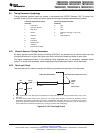
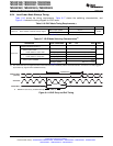
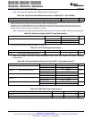
6.9 General-Purpose Input/Output (GPIO)
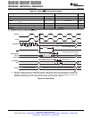
6.9.1 GPIO - Output Timing
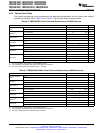
Table 6-14. General-Purpose Output Switching Characteristics
PARAMETER MIN MAX UNIT
t
r(GPO)
Rise time, GPIO switching low to high All GPIOs 8 ns
t
f(GPO)
Fall time, GPIO switching high to low All GPIOs 8 ns
t
fGPO
Toggling frequency, GPO pins 25 MHz
Figure 6-11. General-Purpose Output Timing
Copyright © 2003–2009, Texas Instruments Incorporated Electrical Specifications 109
Submit Documentation Feedback
Product Folder Link(s): TMS320F2809 TMS320F2808 TMS320F2806 TMS320F2802 TMS320F2801 TMS320C2802
TMS320C2801 TMS320F28016 TMS320F28015