


TMS320F2809, TMS320F2808, TMS320F2806
TMS320F2802, TMS320F2801, TMS320C2802
TMS320C2801, TMS320F28016, TMS320F28015
www.ti.com
SPRS230L–OCTOBER 2003–REVISED DECEMBER 2009
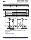
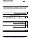
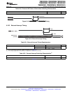
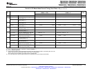
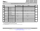
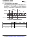
Table 6-35. SPI Master Mode External Timing (Clock Phase = 1)
(1) (2) (3) (4) (5)
SPI WHEN (SPIBRR + 1) IS EVEN OR SPI WHEN (SPIBRR + 1) IS ODD AND
SPIBRR = 0 OR 2 SPIBRR > 3
NO. UNIT
MIN MAX MIN MAX
1 t
c(SPC)M
Cycle time, SPICLK 4t
c(LCO)
128t
c(LCO)
5t
c(LCO)
127t
c(LCO)
ns
t
w(SPCH)M
Pulse duration, SPICLK high 0.5t
c(SPC)M
– 10 0.5t
c(SPC)M
0.5t
c(SPC)M
– 0.5t
c (LCO)
– 10 0.5t
c(SPC)M
– 0.5t
c(LCO)
(clock polarity = 0)
2 ns
t
w(SPCL))M
Pulse duration, SPICLK low 0.5t
c(SPC)M
– 10 0.5t
c(SPC)M
0.5t
c(SPC)M
– 0.5t
c (LCO)
– 10 0.5t
c(SPC)M
– 0.5t
c(LCO
(clock polarity = 1)
t
w(SPCL)M
Pulse duration, SPICLK low 0.5t
c(SPC)M
– 10 0.5t
c(SPC)M
0.5t
c(SPC)M
+ 0.5t
c(LCO)
– 10 0.5t
c(SPC)M
+ 0.5t
c(LCO)
(clock polarity = 0)
3 ns
t
w(SPCH)M
Pulse duration, SPICLK high 0.5t
c(SPC)M
– 10 0.5t
c(SPC)M
0.5
tc(SPC)M
+ 0.5t
c(LCO)
– 10 0.5t
c(SPC)M
+ 0.5t
c(LCO)
(clock polarity = 1)
t
su(SIMO-SPCH)M
Setup time, SPISIMO data valid 0.5t
c(SPC)M
– 10 0.5t
c(SPC)M
– 10
before SPICLK high
(clock polarity = 0)
6 ns
t
su(SIMO-SPCL)M
Setup time, SPISIMO data valid 0.5t
c(SPC)M
– 10 0.5t
c(SPC)M
– 10
before SPICLK low
(clock polarity = 1)
t
v(SPCH-SIMO)M
Valid time, SPISIMO data valid after 0.5t
c(SPC)M
– 10 0.5t
c(SPC)M
– 10
SPICLK high (clock polarity = 0)
7 ns
t
v(SPCL-SIMO)M
Valid time, SPISIMO data valid after 0.5t
c(SPC)M
– 10 0.5t
c(SPC)M
– 10
SPICLK low (clock polarity = 1)
t
su(SOMI-SPCH)M
Setup time, SPISOMI before 35 35
SPICLK high (clock polarity = 0)
10 ns
t
su(SOMI-SPCL)M
Setup time, SPISOMI before 35 35
SPICLK low (clock polarity = 1)
t
v(SPCH-SOMI)M
Valid time, SPISOMI data valid after 0.25t
c(SPC)M
– 10 0.5t
c(SPC)M
– 10
SPICLK high (clock polarity = 0)
11 ns
t
v(SPCL-SOMI)M
Valid time, SPISOMI data valid after 0.25
tc(SPC)M
– 10 0.5
tc(SPC)M
– 10
SPICLK low (clock polarity = 1)
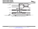
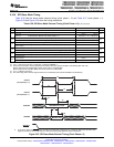
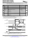
(1) The MASTER/SLAVE bit (SPICTL.2) is set and the CLOCK PHASE bit (SPICTL.3) is set.
(2) t
c(SPC)
= SPI clock cycle time = LSPCLK/4 or LSPCLK/(SPIBRR + 1)
(3) Internal clock prescalers must be adjusted such that the SPI clock speed is limited to the following SPI clock rate:
Master mode transmit 25 MHz MAX, master mode receive 12.5 MHz MAX
Slave mode transmit 12.5 MHz MAX, slave mode receive 12.5 MHz MAX.
(4) t
c(LCO)
= LSPCLK cycle time
(5) The active edge of the SPICLK signal referenced is controlled by the CLOCK POLARITY bit (SPICCR.6).
Copyright © 2003–2009, Texas Instruments Incorporated Electrical Specifications 121
Submit Documentation Feedback
Product Folder Link(s): TMS320F2809 TMS320F2808 TMS320F2806 TMS320F2802 TMS320F2801 TMS320C2802
TMS320C2801 TMS320F28016 TMS320F28015