


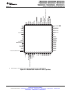
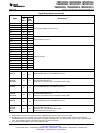
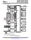
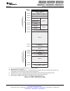
INT[12:1]
Real-Time JTAG
(TDI, TDO, TRST
, TCK,
TMS, EMU0, EMU1)
C28x CPU
(100 MHz)
NMI
, INT13
Memory Bus
INT14
SYSCLKOUT
RS
CLKIN
12-Bit ADC
ADCSOCA/B
SOCA/B
16 Channels
12
6
32
XCLKOUT
XRS
XCLKIN
X1
X2
32
System Control
(Oscillator, PLL,
Peripheral Clocking,
Low-Power Modes,
Watchdog)
ePWM1/2/3/4/5/6
(12 PWM outputs,
6 trip zones,
6 timers 16-bit)
eCAP1/2/3/4
(4 timers 32-bit)
eQEP1/2
eCAN-A/B (32 mbox)
External Interrupt
Control
PIE
(96 Interrupts)
(A)
FIFO
FIFO
FIFO
SCI-A/B
SPI-A/B/C/D
I
2
C-A
4
8
4
2
16
4
GPIO MUX
GPIOs
(35)
TINT0
TINT1
TINT2
7
Peripheral Bus
M0 SARAM
1K x 16
M1 SARAM
1K x 16
Boot ROM
4K x 16
(1-wait state)
L0 SARAM
4K x 16
(0-wait)
L1 SARAM
4K x 16
(0-wait)
(B)
H0 SARAM
8K x 16
(0-wait)
(C)
ROM
32K x 16 (C2802)
16K x 16 (C2801)
FLASH
128K x 16 (F2809)
64K x 16 (F2808)
32K x 16 (F2806)
32K x 16 (F2802)
16K x 16 (F2801)
16K x 16 (F2801x)
OTP
1K x 16
(D)
Protected by the code-security module.
32-bit CPU TIMER 0
32-bit CPU TIMER 1
32-bit CPU TIMER 2
TMS320F2809, TMS320F2808, TMS320F2806
TMS320F2802, TMS320F2801, TMS320C2802
TMS320C2801, TMS320F28016, TMS320F28015
www.ti.com
SPRS230L–OCTOBER 2003–REVISED DECEMBER 2009
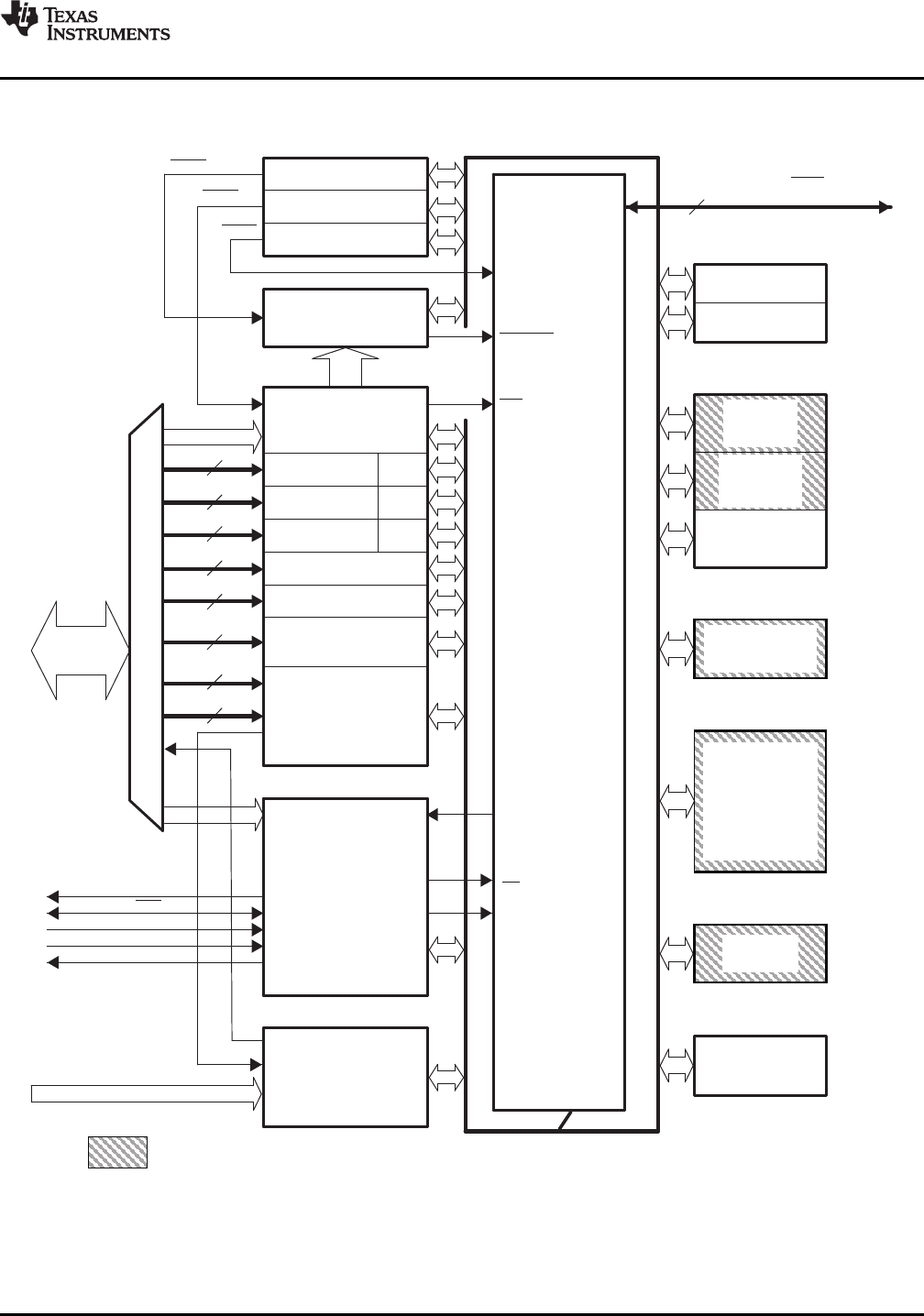
3 Functional Overview
A. 43 of the possible 96 interrupts are used on the devices.
B. Not available in F2802, F2801, C2802, and C2801.
C. Not available in F2806, F2802, F2801, C2802, and C2801.
D. The 1K x 16 OTP has been replaced with 1K x 16 ROM for C280x devices.
Figure 3-1. Functional Block Diagram
Copyright © 2003–2009, Texas Instruments Incorporated Functional Overview 25
Submit Documentation Feedback
Product Folder Link(s): TMS320F2809 TMS320F2808 TMS320F2806 TMS320F2802 TMS320F2801 TMS320C2802
TMS320C2801 TMS320F28016 TMS320F28015