


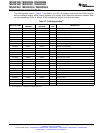
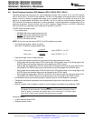

Baud rate =
LSPCLK
4
LSPCLK
(SPIBRR ) 1)
when SPIBRR = 3 to 127
Baud rate = when SPIBRR = 0,1, 2
TMS320F2809, TMS320F2808, TMS320F2806
TMS320F2802, TMS320F2801, TMS320C2802
TMS320C2801, TMS320F28016, TMS320F28015
SPRS230L–OCTOBER 2003–REVISED DECEMBER 2009
www.ti.com
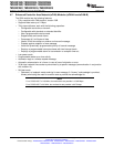
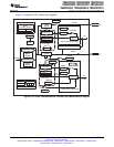
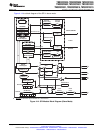
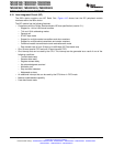
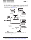
4.9 Serial Peripheral Interface (SPI) Modules (SPI-A, SPI-B, SPI-C, SPI-D)
The 280x devices include the four-pin serial peripheral interface (SPI) module. Up to four SPI modules
(SPI-A, SPI-B, SPI-C, and SPI-D) are available. The SPI is a high-speed, synchronous serial I/O port that
allows a serial bit stream of programmed length (one to sixteen bits) to be shifted into and out of the
device at a programmable bit-transfer rate. Normally, the SPI is used for communications between the
DSP controller and external peripherals or another processor. Typical applications include external I/O or
peripheral expansion through devices such as shift registers, display drivers, and ADCs. Multidevice
communications are supported by the master/slave operation of the SPI.
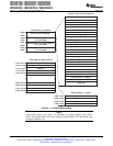
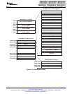
The SPI module features include:
• Four external pins:
– SPISOMI: SPI slave-output/master-input pin
– SPISIMO: SPI slave-input/master-output pin
– SPISTE: SPI slave transmit-enable pin
– SPICLK: SPI serial-clock pin
NOTE: All four pins can be used as GPIO, if the SPI module is not used.
• Two operational modes: master and slave
Baud rate: 125 different programmable rates.
• Data word length: one to sixteen data bits
• Four clocking schemes (controlled by clock polarity and clock phase bits) include:
– Falling edge without phase delay: SPICLK active-high. SPI transmits data on the falling edge of the
SPICLK signal and receives data on the rising edge of the SPICLK signal.
– Falling edge with phase delay: SPICLK active-high. SPI transmits data one half-cycle ahead of the
falling edge of the SPICLK signal and receives data on the falling edge of the SPICLK signal.
– Rising edge without phase delay: SPICLK inactive-low. SPI transmits data on the rising edge of the
SPICLK signal and receives data on the falling edge of the SPICLK signal.
– Rising edge with phase delay: SPICLK inactive-low. SPI transmits data one half-cycle ahead of the
falling edge of the SPICLK signal and receives data on the rising edge of the SPICLK signal.
• Simultaneous receive and transmit operation (transmit function can be disabled in software)
• Transmitter and receiver operations are accomplished through either interrupt-driven or polled
algorithms.
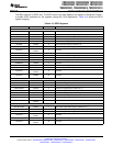
• Nine SPI module control registers: Located in control register frame beginning at address 7040h.
NOTE
All registers in this module are 16-bit registers that are connected to Peripheral Frame 2.
When a register is accessed, the register data is in the lower byte (7–0), and the upper
byte (15–8) is read as zeros. Writing to the upper byte has no effect.
Enhanced feature:
• 16-level transmit/receive FIFO
• Delayed transmit control
76 Peripherals Copyright © 2003–2009, Texas Instruments Incorporated
Submit Documentation Feedback
Product Folder Link(s): TMS320F2809 TMS320F2808 TMS320F2806 TMS320F2802 TMS320F2801 TMS320C2802
TMS320C2801 TMS320F28016 TMS320F28015