


TMS320F2809, TMS320F2808, TMS320F2806
TMS320F2802, TMS320F2801, TMS320C2802
TMS320C2801, TMS320F28016, TMS320F28015
www.ti.com
SPRS230L–OCTOBER 2003–REVISED DECEMBER 2009
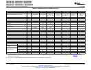
List of Figures
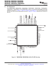
2-1 TMS320F2809, TMS320F2808 100-Pin PZ LQFP (Top View) ............................................................ 15
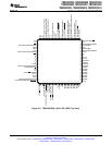
2-2 TMS320F2806 100-Pin PZ LQFP (Top View)................................................................................ 16
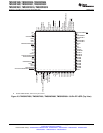
2-3 TMS320F2802, TMS320F2801, TMS320C2802, TMS320C2801 100-Pin PZ LQFP (Top View) ..................... 17
2-4 TMS320F2801x 100-Pin PZ LQFP (Top View) .............................................................................. 18
2-5 TMS320F2809, TMS320F2808, TMS320F2806,TMS320F2802, TMS320F2801,
TMS320F28016, TMS320F28015, TMS320C2802, TMS320C2801
100-Ball GGM and ZGM MicroStar BGA™ (Bottom View) ................................................................. 18
3-1 Functional Block Diagram ....................................................................................................... 26
3-2 F2809 Memory Map.............................................................................................................. 27
3-3 F2808 Memory Map.............................................................................................................. 28
3-4 F2806 Memory Map.............................................................................................................. 29
3-5 F2802, C2802 Memory Map .................................................................................................... 30
3-6 F2801, F28015, F28016, C2801 Memory Map............................................................................... 30
3-7 External and PIE Interrupt Sources............................................................................................ 44
3-8 Multiplexing of Interrupts Using the PIE Block ............................................................................... 44
3-9 Clock and Reset Domains ...................................................................................................... 46
3-10 OSC and PLL Block Diagram................................................................................................... 47
3-11 Using a 3.3-V External Oscillator............................................................................................... 48
3-12 Using a 1.8-V External Oscillator............................................................................................... 48
3-13 Using the Internal Oscillator .................................................................................................... 48
3-14 Watchdog Module ................................................................................................................ 51
4-1 CPU-Timers....................................................................................................................... 53
4-2 CPU-Timer Interrupt Signals and Output Signal ............................................................................. 54
4-3 Multiple PWM Modules in a 280x System .................................................................................... 55
4-4 ePWM Sub-Modules Showing Critical Internal Signal Interconnections .................................................. 57
4-5 eCAP Functional Block Diagram ............................................................................................... 59
4-6 eQEP Functional Block Diagram............................................................................................... 61
4-7 Block Diagram of the ADC Module ............................................................................................ 64
4-8 ADC Pin Connections With Internal Reference .............................................................................. 65
4-9 ADC Pin Connections With External Reference ............................................................................. 66
4-10 eCAN Block Diagram and Interface Circuit ................................................................................... 69
4-11 eCAN-A Memory Map ........................................................................................................... 70
4-12 eCAN-B Memory Map ........................................................................................................... 71
4-13 Serial Communications Interface (SCI) Module Block Diagram............................................................ 75
4-14 SPI Module Block Diagram (Slave Mode) .................................................................................... 79
4-15 I2C Peripheral Module Interfaces .............................................................................................. 81
4-16 GPIO MUX Block Diagram...................................................................................................... 82
4-17 Qualification Using Sampling Window......................................................................................... 85
5-1 Example of TMS320x280x/2801x Device Nomenclature ................................................................... 87
6-1 Typical Operational Current Versus Frequency (F2808) .................................................................. 100
6-2 Typical Operational Power Versus Frequency (F2808).................................................................... 100
6-3 Typical Operational Current Versus Frequency (C280x) .................................................................. 101
6-4 Typical Operational Power Versus Frequency (C280x) ................................................................... 101
6-5 Emulator Connection Without Signal Buffering for the DSP .............................................................. 102
6-6 3.3-V Test Load Circuit......................................................................................................... 103
6-7 Clock Timing..................................................................................................................... 106
6-8 Power-on Reset................................................................................................................. 107
Copyright © 2003–2009, Texas Instruments Incorporated List of Figures 5