


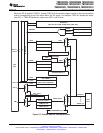
PLL
X1
X2
Power
Modes
Control
Watchdog
Block
28x
CPU
Peripheral Bus
Low-Speed Peripherals
SCI-A/B, SPI-A/B/C/D
Peripheral
Registers
High-Speed Prescaler
Low-Speed Prescaler
Clock Enables
GPIO
MUX
System
Control
Registers
XCLKIN
ADC
Registers
12-Bit ADC
16 ADC inputs
LSPCLK
I/O
Peripheral Reset
SYSCLKOUT
(A)
XRS
Reset
GPIOs
Peripheral
Registers
I/O
OSC
CLKIN
(A)
HSPCLK
eCAN-A/B
I
2
C-A
Peripheral
Registers
I/O
ePWM 1/2/3/4/5/6
eCAP 1/2/3/4 eQEP 1/2
Peripheral
Registers
CPU
Timers
TMS320F2809, TMS320F2808, TMS320F2806
TMS320F2802, TMS320F2801, TMS320C2802
TMS320C2801, TMS320F28016, TMS320F28015
SPRS230L–OCTOBER 2003–REVISED DECEMBER 2009
www.ti.com
Each external interrupt can be enabled/disabled or qualified using positive, negative, or both positive and
negative edge. For more information, see the TMS320x280x, 2801x, 2804x DSP System Control and
Interrupts Reference Guide (literature number SPRU712).
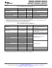
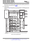
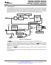
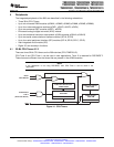
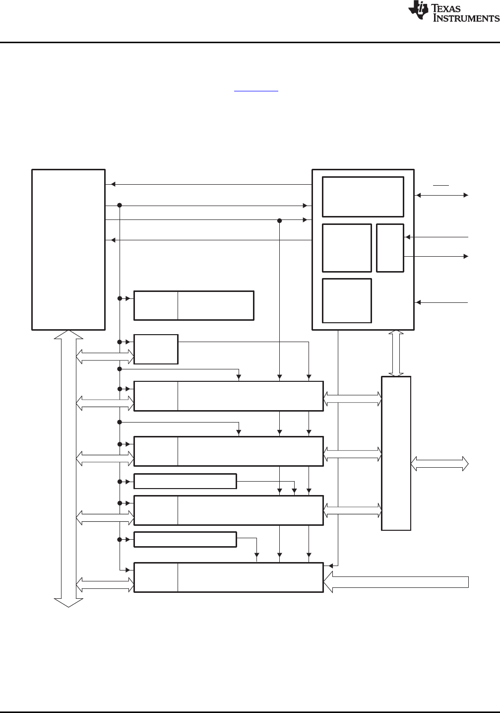
3.6 System Control
This section describes the 280x oscillator, PLL and clocking mechanisms, the watchdog function and the
low power modes. Figure 3-9 shows the various clock and reset domains in the 280x devices that will be
discussed.
A. CLKIN is the clock into the CPU. It is passed out of the CPU as SYSCLKOUT (that is, CLKIN is the same frequency
as SYSCLKOUT).
Figure 3-9. Clock and Reset Domains
46 Functional Overview Copyright © 2003–2009, Texas Instruments Incorporated
Submit Documentation Feedback
Product Folder Link(s): TMS320F2809 TMS320F2808 TMS320F2806 TMS320F2802 TMS320F2801 TMS320C2802
TMS320C2801 TMS320F28016 TMS320F28015