


Assembly-Level Troubleshooting with Block Diagrams ESG Family Signal Generators
Before You Begin Troubleshooting
2-2 Service Guide
Before You Begin Troubleshooting
Be sure to review the warning and caution statements described in Chapter 7 prior to
troubleshooting your signal generator.
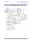
Using this Chapter with Service Software
Some block diagrams in this chapter are accompanied by a table for use with the
automated service software that came with your signal generator. These tables list the
signal generator’s test conditions and the expected ABUS node voltages. The service
software has a utility program which measures and displays the node voltages for each
test. Refer to your signal generator’s calibration guide for information on using the
software.
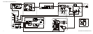
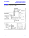
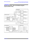
The block diagrams and ABUS node tables are arranged in the following order:
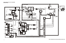
A5 Dual Arbitrary Waveform Generator Block Diagram (Option UND)
A6 Bit Error Rate Test Block Diagram (Option UN7)
A7 Baseband Generator Block Diagram (Options UN3 & UN4)
A7 DBMIC Baseband Generator Block Diagram (Options UN8 & UN9)
A8 Data Generator Block Diagram (Options UN3 & UN4)
A8 Data Generator - Rev. A & B Block Diagram (Options UN8 & UN9)
A8 Flex Data Generator - Rev. C & D Block Diagram (Options UN8 & UN9)
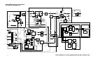
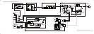
A9 Output ABUS Nodes (ESG-A Series)
A9 Output Block Diagram (ESG-A Series)
A9 Output ABUS Nodes (ESG-D Series)
A9 Output ABUS Nodes (ESG-AP, & ESG-DP Series)
A9 Output Block Diagram (ESG-D, ESG-AP, & ESG-DP Series)
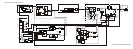
A11 Reference ABUS Nodes (ESG-A & ESG-D Series)
A11 Reference Block Diagram (ESG-A & ESG-D Series)
A11 Reference ABUS Nodes (ESG-AP & ESG-DP Series)
A11 Reference Block Diagram (ESG-AP & ESG-DP Series)
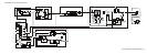
A12 Synthesizer/Doubler ABUS Nodes (ESG-A & ESG-D Series)
A12 Synthesizer/Doubler Block Diagram (ESG-A & ESG-D Series)
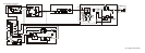
A14 CPU/Motherboard ABUS Nodes