


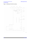
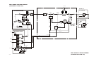

ESG Family Signal Generators Initial Troubleshooting and RF Block Diagrams
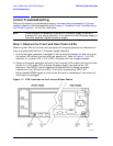
Initial Troubleshooting
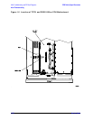
Service Guide 1-17
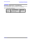
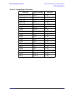
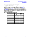
Table 1-3 Voltage Supply Tolerances
Test Point Supply Voltage Tolerance
J6 (pins 2, 3, 12, 13) +5.2 V +/− 3%
J6 (pin 20) +15 V +/− 3%
J6 (pin 18) −15 V +/− 3%
J6 (pin 19) +12 V +/− 3%
J6 (pin 17) +15 V_STBY +/− 5%
TP301 DGND N/A
TP302 +5.2 V +/− 3%
TP501 +10 V_REF +/− 3%
TP502 +15 V +/− 3%
TP503 −15 V +/− 3%
TP504 +32 V +/− 4%
TP505 +12 V +/− 3%
TP506 +5.2 VD +/− 4%
TP507 +9 V +/− 4%
TP508 −6 V +/− 4%
TP509 −5.2 V +/− 4%
TP510 +12.5 V +/− 4%
TP511 −12.5 V +/− 4%