


Initial Troubleshooting and RF Block Diagrams ESG Family Signal Generators
Initial Troubleshooting
1-16 Service Guide
Step 5: Measure the Individual Voltage Supplies
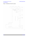
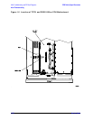
The voltages supplied as inputs from the power supply via J6 to the motherboard are
+15 V (TP502), +15 V standby (+15 V_STBY), −15 V (TP503), +12 V (TP505), and
+5.2 V (TP302). DGND (TP301) is associated with these supplies.
The −6 V (TP508) and −5.2 V (TP509) supplies receive their input from the +5.2 V digital
supply (5.2 VD at TP506). The +5.2 V digital line is filtered to prevent the switching power
supply noise from being induced onto the +5.2 VD supply lines. The −6 V is a bias voltage
for circuits on the output board and other RF circuitry. The −5.2 V is used by the emitter
coupled logic (ECL) digital ICs. The LCD display driver voltage (VLCD), a −14 V to −24 V
source, also receives input from the +5.2 VD supply.
The input to the +32 V supply (TP504) is the +12 V supply. The +32 V supply is used by the
synthesizer/doubler assembly. This supply also includes an LC noise filter.
The +12.5 V regulated supply (TP510) originates from the +15 V input. The −12.5 V
regulated supply (TP511) originates from the −15 V input. These two supplies are used by
the solid-state attenuator and the reverse power protection (RPP). The +10 V reference
(TP501) originates from the +15 V input. The +9 V supply (TP507) originates from the
+10 V reference and the +12 V supply.
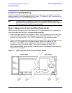
1. Unplug the signal generator and turn it upside-down.
2. Expose the motherboard by removing the bottom cover. It is secured by 15 screws.
3. Plug in the signal generator.
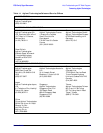
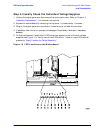
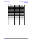
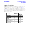
4. Measure the voltage of each supply to verify they are within the tolerances listed in
Table 1-3. The voltage supply test point locations are shown in Figure 1-4. If all the
voltages are within tolerance, proceed to “Step 7: Check for Basic CPU Functionality”.