


TMS320C6202
FIXED-POINT DIGITAL SIGNAL PROCESSOR
SPRS072B – AUGUST 1998 – REVISED AUGUST 1999
28
POST OFFICE BOX 1443 • HOUSTON, TEXAS 77251–1443
absolute maximum ratings over operating case temperature range (unless otherwise noted)
†
Supply voltage range, CV
DD
(see Note 1) – 0.3 V to 2.3 V. . . . . . . . . . . . . . . . . . . . . . . . . . . . . . . . . . . . . . . . . . .
Supply voltage range, DV
DD
(see Note 1) –0.3 V to 4 V. . . . . . . . . . . . . . . . . . . . . . . . . . . . . . . . . . . . . . . . . . . . .
Input voltage range –0.3 V to 4 V. . . . . . . . . . . . . . . . . . . . . . . . . . . . . . . . . . . . . . . . . . . . . . . . . . . . . . . . . . . . . . . . .
Output voltage range –0.3 V to 4 V. . . . . . . . . . . . . . . . . . . . . . . . . . . . . . . . . . . . . . . . . . . . . . . . . . . . . . . . . . . . . . .
Operating case temperature range, T
C
0 C to 90 C. . . . . . . . . . . . . . . . . . . . . . . . . . . . . . . . . . . . . . . . . . . . .
Storage temperature range, T
stg
–55 C to 150 C. . . . . . . . . . . . . . . . . . . . . . . . . . . . . . . . . . . . . . . . . . . . . . .
†
Stresses beyond those listed under “absolute maximum ratings” may cause permanent damage to the device. These are stress ratings only, and
functional operation of the device at these or any other conditions beyond those indicated under “recommended operating conditions” is not
implied. Exposure to absolute-maximum-rated conditions for extended periods may affect device reliability.
NOTE 1: All voltage values are with respect to V
SS
.
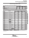
recommended operating conditions
MIN NOM MAX UNIT
CV
DD
Supply voltage 1.71 1.8 1.89 V
DV
DD
Supply voltage 3.14 3.30 3.46 V
V
SS
Supply ground 0 0 0 V
V
IH
High-level input voltage 2.0 V
V
IL
Low-level input voltage 0.8 V
I
OH
High-level output current –8 mA
I
OL
Low-level output current 8 mA
T
C
Operating case temperature 0 90 C
electrical characteristics over recommended ranges of supply voltage and operating case
temperature (unless otherwise noted)
PARAMETER TEST CONDITIONS MIN TYP MAX UNIT
V
OH
High-level output voltage DV
DD
= MIN, I
OH
= MAX 2.4 V
V
OL
Low-level output voltage DV
DD
= MIN, I
OL
= MAX 0.6 V
I
I
Input current
‡
V
I
= V
SS
to DV
DD
±10 uA
I
OZ
Off-state output current V
O
= DV
DD
or 0 V ±10 uA
I
DD2V
Supply current, CPU + CPU memory access
§
CV
DD
= NOM, CPU clock = 200 MHz TBD mA
I
DD2V
Supply current, peripherals
¶
CV
DD
= NOM, CPU clock = 200 MHz TBD mA
I
DD3V
Supply current, I/O pins
#
DV
DD
= NOM, CPU clock = 200 MHz TBD mA
C
i
Input capacitance 10 pF
C
o
Output capacitance 10 pF
‡
TMS and TDI are not included due to internal pullups. TRST is not included due to internal pulldown.
§
Measured with average CPU activity:
50% of time: 8 instructions per cycle, 32-bit DMEM access per cycle
50% of time: 2 instructions per cycle, 16-bit DMEM access per cycle
¶
Measured with average peripheral activity:
50% of time: Timers at max rate
McBSPs at E1 rate
DMA burst transfer between DMEM and SDRAM
50% of time: Timers at max rate
McBSPs at E1 rate
DMA servicing McBSPs
#
Measured with average I/O activity (30-pF load, SDCLK on):
25% of time: Reads from external SDRAM
25% of time: Writes to external SDRAM
50% of time: No activity
ADVANCE INFORMATION