


TMS320C6202
FIXED-POINT DIGITAL SIGNAL PROCESSOR
SPRS072B – AUGUST 1998 – REVISED AUGUST 1999
13
POST OFFICE BOX 1443 • HOUSTON, TEXAS 77251–1443
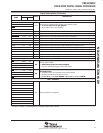
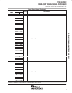
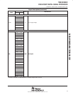
Signal Descriptions (Continued)
SIGNAL
PIN NO.
TYPE
†
DESCRIPTION
NAME
GJL GLS
TYPE
†
DESCRIPTION
EXPANSION BUS (CONTINUED)
XBE3/XA5 C7 C5
XBE2/XA4 D8 A4
I/O/Z
Expansion bus multiplexed byte-enable control/address signals
• Act as byte enable for host
p
ort o
p
eration
XBE1/XA3 A6 B5
I/O/Z
•
A
c
t
as
b
y
t
e ena
bl
e
f
or
h
os
t
por
t
opera
ti
on
• Act as address for I/O port operation
XBE0/XA2 C8 C6
• Act
as
address
for
I/O
ort
o eration
XOE A7 A6 O/Z Expansion bus I/O port output enable
XRE C9 C7 O/Z Expansion bus I/O port read enable
XWE/XWAIT D10 B7 O/Z Expansion bus I/O port write enable and host port wait signals
XCS A10 C9 I Expansion bus host port chip-select input
XAS D9 B6 I/O/Z Expansion bus host port address strobe
XCNTL B10 B9 I Expansion bus host control. XCNTL selects between expansion bus address or data register
XW/R D11 B8 I/O/Z Expansion bus host port write/read enable. XW/R polarity selected at reset
XRDY A5 C4 I/O/Z Expansion bus host port ready (active low) and I/O port ready (active high)
XBLAST B6 B4 I/O/Z Expansion bus host port burst last–polarity selected at reset
XBOFF B11 A10 I Expansion bus back off
XHOLD B5 A2 I/O/Z Expansion bus hold request
XHOLDA D7 B3 I/O/Z Expansion bus hold acknowledge
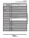
EMIF – CONTROL SIGNALS COMMON TO ALL TYPES OF MEMORY
CE3 AB25 Y21
CE2 AA24 W20
O/Z
Memory space enables
• Enabled by bits 24 and 25 of the word address
CE1 AB26 AA22
O/Z
•
E
na
bl
e
d
b
y
bit
s
24
an
d
25
o
f
th
e wor
d
a
dd
ress
•
O
nl
y
on
e
asse
rt
ed
du
rin
g
a
n
y
e
xt
e
rn
a
l
da
t
a
access
CE0 AA25 W21
• Only
one
asserted
during
any
external
data
access
BE3 Y24 V20
Byte-enable control
BE2 W23 V21
O/Z
Byte
-
enable
control
• Decoded from the two lowest bits of the internal address
BE1 AA26 W22
O/Z
• Byte-write enables for most types of memory
C b di tl t d t SDRAM d d it k i l (SDQM)
BE0 Y25 U20
• Can be directly connected to SDRAM read and write mask signal (SDQM)
EMIF – ADDRESS
EA21 J25 H20
EA20 J26 H21
EA19 L23 H22
EA18 K25 J20
EA17 L24 J21
EA16 L25 K21
O/Z External address (word address)
EA15 M23 K20
EA14 M24 K22
EA13 M25 L21
EA12 N23 L20
EA11 P24 L22
†
I = Input, O = Output, Z = High Impedance, S = Supply Voltage, GND = Ground
ADVANCE INFORMATION