


TMS320C6202
FIXED-POINT DIGITAL SIGNAL PROCESSOR
SPRS072B – AUGUST 1998 – REVISED AUGUST 1999
11
POST OFFICE BOX 1443 • HOUSTON, TEXAS 77251–1443
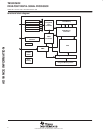
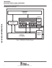
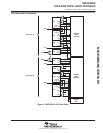
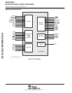
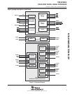
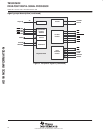
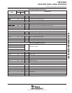
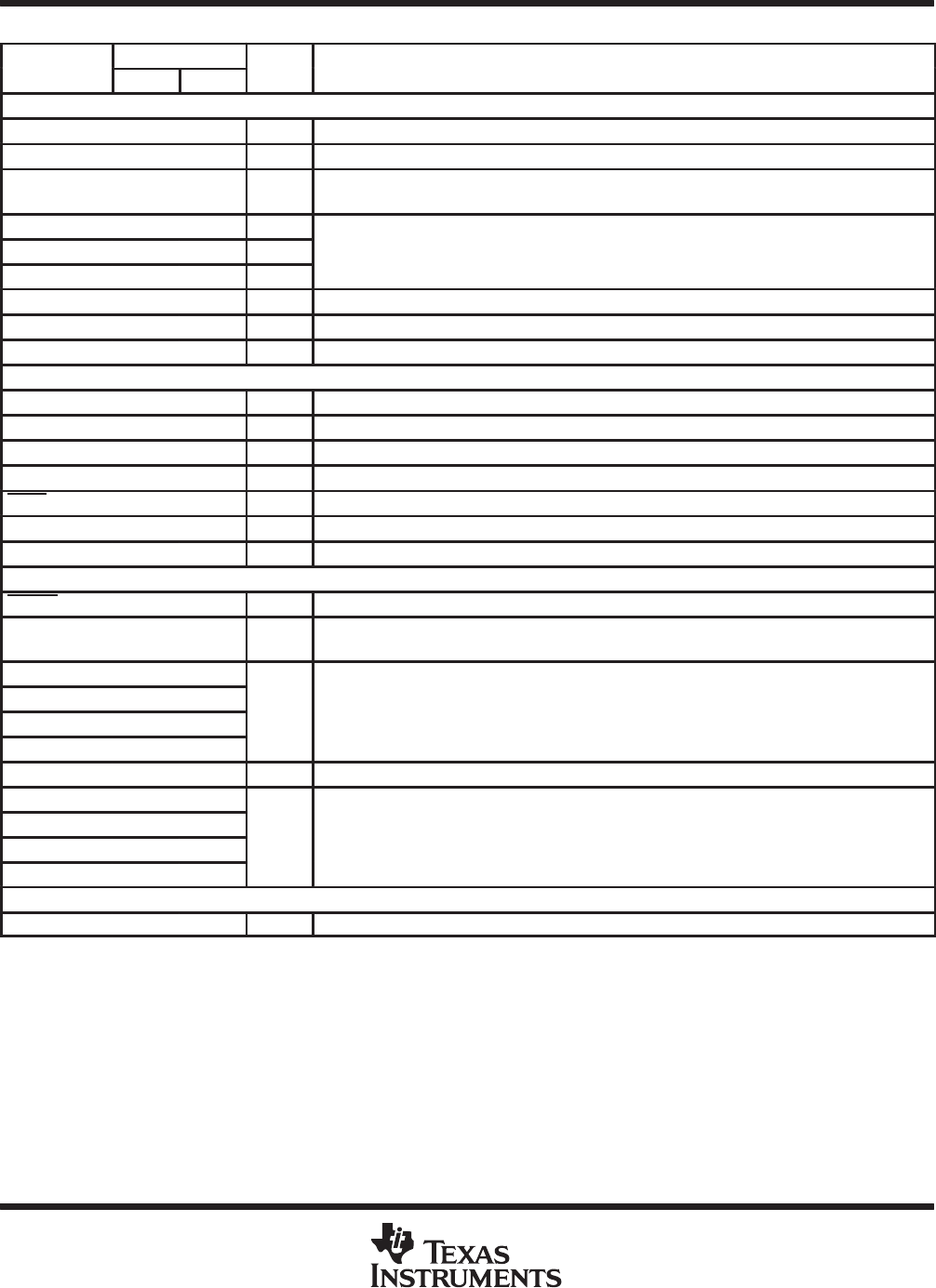
Signal Descriptions
SIGNAL
PIN NO.
TYPE
†
DESCRIPTION
NAME
GJL GLS
TYPE
†
DESCRIPTION
CLOCK/PLL
CLKIN C12 B10 I Clock Input
CLKOUT1 AD20 Y18 O Clock output at full device speed
CLKOUT2 AC19 AB19 O
Clock output at half of device speed
• Used for synchronous memory interface
CLKMODE0 B15 B12 I
Cl k d l t (N t CLKMODE1 d CLKMODE2 l t f GLS d i l )
CLKMODE1 – A9 I
Clock mode selects (Note: CLKMODE1 and CLKMODE2 selects are for GLS devices only)
• Selects whether the CPU clock frequency = in
p
ut clock frequency x4 or x1
CLKMODE2 – A14 I
• Selects
whether
the
CPU
clock
frequency
=
in ut
clock
frequency
x4
or
x1
PLLV
‡
D13 C11 A
§
PLL analog V
CC
connection for the low-pass filter
PLLG
‡
D14 C12 A
§
PLL analog GND connection for the low-pass filter
PLLF C13 A11 A
§
PLL low-pass filter connection to external components and a bypass capacitor
JTAG EMULATION
TMS AD7 Y5 I JTAG test-port mode select (features an internal pullup)
TDO AE6 AA4 O/Z JTAG test-port data out
TDI AF5 Y4 I JTAG test-port data in (features an internal pullup)
TCK AE5 AB2 I JTAG test-port clock
TRST AC7 AA3 I JTAG test-port reset (features an internal pulldown)
EMU1 AF6 AA5 I/O/Z Emulation pin 1, pullup with a dedicated 20-kΩ resistor
¶
EMU0 AC8 AB4 I/O/Z Emulation pin 0, pullup with a dedicated 20-kΩ resistor
¶
RESET AND INTERRUPTS
RESET K2 J3 I Device reset
NMI L2 K2 I
Nonmaskable interrupt
• Edge-driven (rising edge)
EXT_INT7 V4 U2
EXT_INT6 Y2 U3
I
External interrupts
EXT_INT5 AA1 W1
I
• Edge-driven (rising edge)
EXT_INT4 W4 V2
IACK Y1 V1 O Interrupt acknowledge for all active interrupts serviced by the CPU
INUM3 V2 R3
INUM2 U4 T1
O
Active interrupt identification number
• Valid during IACK for all active interru
p
ts (not just external)
INUM1 V3 T2
O
•
V
a
lid
d
ur
i
ng
IACK
f
or a
ll
ac
ti
ve
i
n
t
errup
t
s
(
no
t
j
us
t
ex
t
erna
l)
• En
c
o
d
in
g
or
de
r follow
s
th
e
int
e
rr
u
pt-
se
rvi
ce
f
e
t
c
h-p
ac
k
e
t or
de
rin
g
INUM0 W2 T3
• Encoding
order
follows
the
interru t service
fetch acket
ordering
POWER-DOWN STATUS
PD AB2 Y2 O Power-down modes 2 or 3 (active if high)
†
I = Input, O = Output, Z = High Impedance, S = Supply Voltage, GND = Ground
‡
PLLV and PLLG are not part of external voltage supply or ground. See the
clock PLL
section for information on how to connect these pins.
§
A = Analog Signal (PLL Filter)
¶
For emulation and normal operation, pull up EMU1 and EMU0 with a dedicated 20-kΩ resistor. For boundary scan, pull down EMU1 and EMU0
with a dedicated 20-kΩ resistor.
ADVANCE INFORMATION