


TMS320C6202
FIXED-POINT DIGITAL SIGNAL PROCESSOR
SPRS072B – AUGUST 1998 – REVISED AUGUST 1999
27
POST OFFICE BOX 1443 • HOUSTON, TEXAS 77251–1443
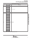
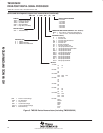
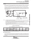
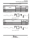
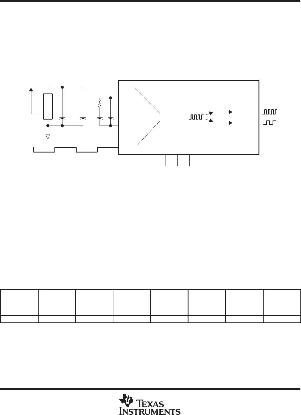
clock PLL
All of the internal ’C6202 clocks are generated from a single source through the CLKIN pin. This source clock
either drives the PLL, which generates the internal CPU clock, or bypasses the PLL to become the CPU clock.
To use the PLL to generate the CPU clock, the filter circuit shown in Figure 6 must be properly designed.
To configure the ’C6202 PLL clock for proper operation, see Figure 6 and Table 3. To minimize the clock jitter,
a single clean power supply should power both the ’C6202 device and the external clock oscillator circuit. The
minimum CLKIN rise and fall times should also be observed. See the
input and output clocks
section for input
clock timing requirements.
CLKIN
PLLV
PLLF
PLLG
CPU Clock
0
1
– MULT×1
– MULT×4
– Reserved
f(CPU Clock)=f(CLKIN)
f(CPU Clock)=f(CLKIN)×4
10 µF 0.1 µF
(Bypass)
C1 C2
R1
’320C6202
3.3 V
GND
2
1 IN
3 OUT
EMI Filter
CLKOUT2÷ 2
CLKOUT1÷ 1
0
0
0
0
All Other Modes
CLKMODE2
CLKMODE1
CLKMODE0
NOTES: A. The ’C6202 PLL can generate CPU clock frequencies in the range of 130 MHz to 250 MHz. For frequencies below 130 MHz, the
PLL should be configured to operate in bypass mode.
B. For the ’C6202, values for C1, C2, and R1 are fixed and apply to all valid frequency ranges of CLKIN and CPU clock frequency.
C. For CLKMODE x1, the PLL is bypassed and all six external PLL components can be removed. For this case, the PLLV terminal
has to be connected to a clean 3.3-V supply and the PLLG and PLLF terminals should be tied together.
D. The 3.3-V supply for the EMI filter (and PLLV) must be from the same 3.3-V power plane supplying the I/O voltage, DV
DD
.
E. EMI filter manufacturer TDK part number ACF451832-153-T
F. CLKMODE2 and CLKMODE1 exist only on the GLS device. There are no equivalent connections on the GJL device.
G. The reserved PLL clock modes (GLS devices only) may or may not be supported on future devices as additional PLL multiply factors.
For future flexibility, a board can be designed so that these inputs are configurable (either through jumpers, switches, or 0-Ω
resistors).
Figure 6. PLL Block Diagram
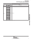
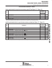
Table 3. TMS320C6202 PLL Component Selection Table
†
CLKMODE
CLKIN
RANGE
(MHz)
CPU CLOCK
FREQUENCY
(CLKOUT1)
RANGE (MHz)
CLKOUT2
RANGE
(MHz)
R1
(Ω)
C1
(nF)
C2
(pF)
TYPICAL
LOCK TIME
(µs)
x4 32.5–62.5 130–250 65–125 60.4 27 560 75
†
Under some operating conditions, the maximum PLL lock time may vary as much as 150% from the specified typical value. For example, if the
typical lock time is specified as 100 µs, the maximum value may be as long as 250 µs.
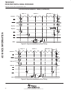
power-supply sequencing
The 1.8-V supply powers the core and the 3.3-V supply powers the I/O buffers. The core supply should be
powered up first, or at the same time as the I/O buffers supply. This is to ensure that the I/O buffers have valid
inputs from the core before the output buffers are powered up, thus preventing bus contention with other chips
on the board.
ADVANCE INFORMATION