


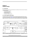

Hardware Design
Dimmable Light Ballast with Power Factor Correction, Rev. 1
30 Freescale Semiconductor
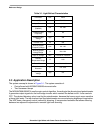
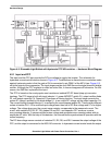
4.2.3 Microcontroller
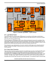
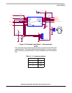
The MC68HC908LB8 microcontroller is the core of the application. It processes the input and feedback
signals and generates appropriate control signals. The description of the pins follows.
The inverter is controlled by signals on the TOP and BOT pins of the MCU.
Signal PWM0 is used to generate a sine wave. This signal (on comparator pin V+) is compared with the
real current (on comparator pin V-) in the on-board comparator. The real current is sensed using the shunt
resistor R4. The signal from PWM0 is filtered in the RC filter comprised of R30, R31 and capacitor C9.
The output of the comparator appears on pin VOUT.
The IRQ pin is used for the zero-crossing detection circuit and for entry to the monitor mode.
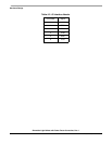
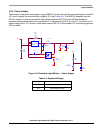
The microcontroller stage incorporates two header connectors, the Luminance Level connector and the
Monitor Mode connector. The Luminance Level connector is used for the Luminance Level potentiometer
(see
Table 4-1). The Monitor Mode connector enables the MCU to enter the Monitor Mode. For Monitor
Mode, the IRQ, OSC1, PTA0, and PTA1 pins are used (see Table 4-2).
The Fault LED is connected to pin PTA5; it indicates the actual state of the application.
DC-bus shift-down voltage is sensed on pin ADC2.
Real currents through tube1 and tube2 are sensed on pins ADC3 and ADC4. The tube voltage difference
is sensed on pin ADC5.
In the discontinuous conduction mode HW variation, PWM1 pin is used directly for switching the PFC
switch transistor (see
Figure A-5). Comparator output is internally connected to the PWM fault pin. In the
hysteresis current control mode HW variation, it is not used.