


TFA9812_2 © NXP B.V. 2009. All rights reserved.
Preliminary data sheet Rev. 02 — 22 January 2009 7 of 66
NXP Semiconductors
TFA9812
BTL stereo Class-D audio amplifier with I
2
S input
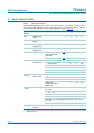
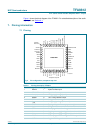
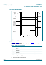
14 OUT2N O Negative PWM output channel 2
15 BOOT1P O Bootstrap high-side driver positive PWM output channel 1
16 OUT1P O Positive PWM output channel 1
17 OUT1P O Positive PWM output channel 1
18 V
DDP
P Positive power supply voltage (8 V to 20 V)
19 V
DDP
P Positive power supply voltage (8 V to 20 V)
20 OUT2P O Positive PWM output channel 2
21 OUT2P O Positive PWM output channel 2
22 BOOT2P O Bootstrap high-side driver positive PWM output channel 2
23 OUT1N O Negative PWM output channel 1
24 OUT1N O Negative PWM output channel 1
25 BOOT1N O Bootstrap high-side driver negative PWM output channel 1
26 V
SSP1
P Negative power supply voltage for channel 1 and channel 2
27 V
SSP1
P Negative power supply voltage for channel 1 and channel 2
28 STAB1 O Decoupling of internal 11 V regulator for channel 1 drivers
29 DIAG O Fault mode indication output (open-drain pin)
30 CDELAY I Timing reference
31 POWERUP I Power-up pin to switch between Sleep and other operational
modes
32 AVOL I Analog volume control (Legacy mode)
33 ENABLE I Enable input to switch between 3-state and other
operational modes
34 GAIN I Gain selection input to select between 0 dB and +24 dB
gain (Legacy mode)
35 CSEL I Control selection input to select between Legacy mode
(no I
2
C bus control) and I
2
C bus control
36 ADSEL2/PLIM2 I Address selection in I
2
C mode input 2, power limiter
selection input 2 in Legacy mode
37 ADSEL1/PLIM1 I Address selection in I
2
C mode input 1, power limiter
selection input 1 in Legacy mode
38 SCL/SFOR I I
2
C bus clock input in I
2
C mode, I
2
S serial data format
selection input in Legacy mode
39 SDA/MS I/O I
2
C bus data input and output in I
2
C mode, master/slave
selection input in Legacy mode
40 V
DDD(3V3)
P Digital supply voltage (3.3 V)
41 STABD O 1.8 V digital stabilizer output
42 REFD P Digital reference voltage
43 TEST2 I Test signal input 2; for test purposes only (connect to V
SS
)
44 DATA I I
2
S bus data input
45 WS I/O I
2
S bus word select input (I
2
S slave mode) or output (I
2
S
master mode)
46 BCK I/O I
2
S bus bit clock input (I
2
S slave mode) or output (I
2
S
master mode)
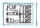
Table 3. Pinning description TFA9812
…continued
Pin Symbol Type Description