


TFA9812_2 © NXP B.V. 2009. All rights reserved.
Preliminary data sheet Rev. 02 — 22 January 2009 26 of 66
NXP Semiconductors
TFA9812
BTL stereo Class-D audio amplifier with I
2
S input
8.7.11 Invalid BCK protection
The BCK clock signal is verified as being at one of the allowed relative frequencies: 32 f
s
,
48 f
s
or 64 f
s
. If it is not at one of these frequencies the TFA9812 will set the output stages
to 3-state mode to prevent audible effects.
The MCLK clock signal is also verified as being valid, see Section 8.2.3.
Detection of violation results in an automatic internal overruling of the MCLK assignment
to BCK.
8.7.12 DC blocking
The TFA9812 features a high pass filter after the I
2
S input to block DC signals. DC values
at the output can damage the peripheral devices. The high pass filter is always enabled.
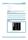
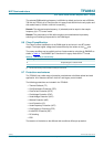
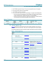
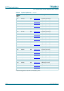
8.7.13 Overview protections
Table 21 shows the overview of the protections.
Table 21. Overview protections
Protections
Symbol Conditions DIAG
pin
I
2
C
flag
[1]
Output Recovering
TF programmable
max. T
j
> 125 °C
Floating - Switching Automatic, increasing
volume control back to
volume setting
OTP T
j
> 160 °C LOW DIAG Floating Automatic, after 1 µs and
T
j
< 160 °C
OCP I
O
> I
ORM
LOW DIAG Floating Automatic, after 1 µs and
I
O
<I
ORM
OVP V
DDA
> 20 V LOW DIAG Floating Restart (fault to operating
when V
DDA
> 8 V and
V
DDA(3V3)
>3V)
UVP V
DDA
< 8 V or
V
DDA(3V3)
<3V
LOW DIAG Floating Restart (fault to operating
when V
DDA
> 8 V and
V
DDA(3V3)
>3V)
ODP T
j
> 140 °C and I
O
>I
ORM
LOW DIAG Floating Restart (fault to operating
when T
j
< 140 °C or
IO < I
ORM
)
WP
[2]
OUTX > V
DDA
− 1 V or
OUTX < REFA + 1 V
LOW DIAG Floating Restart (fault to operating
when OUTX < V
DDA
− 1V
and OUTX > V
SSA
+1V)
LP PLL out of lock Floating LP Floating Restart (fault to operating
when PLL is in lock)
UFP PLL frequency < 45 MHz Floating UFP Floating Restart (fault to operating
when
PLL frequency > 45 MHz)