


TFA9812_2 © NXP B.V. 2009. All rights reserved.
Preliminary data sheet Rev. 02 — 22 January 2009 49 of 66
NXP Semiconductors
TFA9812
BTL stereo Class-D audio amplifier with I
2
S input
[1] C
b
is the total capacitance of one bus line in pF. The maximum capacitive load for each bus line is 400 pF.
[2] After this period, the first clock pulse is generated.
[3] To be suppressed by the input filter.
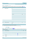
14. Application information
14.1 Output power estimation
The output power just before clipping can be estimated using Equation 10:
(10)
Where:
V
P
= supply voltage (V) (V
DDP
-V
SSP
).
R
L
= load impedance (Ω).
R
DSon
= ‘On’ resistance power switch (Ω).
R
S
= Series resistance output inductor (Ω).
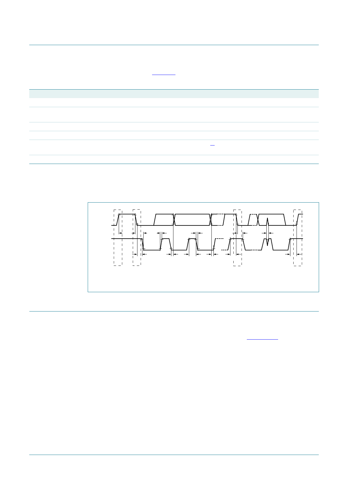
t
SU;STO
set-up time for STOP condition 0.6 - - µs
t
BUF
bus free time between a STOP and
START condition
1.3 - - µs
t
SU;DAT
data set-up time 100 - - ns
t
HD;DAT
data hold time 0 - - µs
t
SP
pulse width of spikes that must be
suppressed by the input filter
[3]
0 - 50 ns
C
b
capacitive load for each bus line - - 400 pF
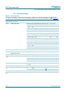
Table 57. Characteristics I
2
C bus interface; see Figure 10
…continued
V
DDD(3V3)
=V
DDA(3V3)
= 2.7 V to 3.6 V; V
DDA
=V
DDP
= 8 V to 20 V;T
amb
=
−
20
°
C to +85
°
C; all voltages referenced to ground;
unless otherwise specified.
Symbol Parameter Conditions Min Typ Max Unit
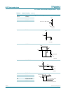
Fig 10. Timing
t
BUF
t
LOW
t
r
t
f
t
HD;STA
t
SU;STA
t
HD;DAT
t
HIGH
t
SU;DAT
t
HD;STA
t
SU;STO
t
SP
P S Sr P
SDA
SCL
010aaa225
P
O
(0.5%)
R
L
R
L
2R
DSon
R
S
+()⋅+
----------------------------------------------------
δ
max
V
P
⋅⋅
2
2R
L
⋅
----------------------------------------------------------------------------------------------
=