


TFA9812_2 © NXP B.V. 2009. All rights reserved.
Preliminary data sheet Rev. 02 — 22 January 2009 28 of 66
NXP Semiconductors
TFA9812
BTL stereo Class-D audio amplifier with I
2
S input
9.3 I
2
C write cycle description
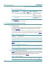
Table 25 shows the cycle required for writing data to the I
2
C registers of the TFA9812. The
byte size is 8 bits. The I
2
C registers of the TFA9812 store two data bytes. Data is always
written in pairs of two bytes. Data transfer is always MSB first.
The cycle format for writing to the TFA9812 using SDA is as follows:
1. The microcontroller asserts a start condition (S).
2. The microcontroller sends the device address (7 bits) of the TFA9812 followed by the
R/!W bit set to 0.
3. The TFA9812 asserts an acknowledge (A).
4. The microcontroller writes the 8-bit TFA9812 register address to which the first data
byte will be written.
5. The TFA9812 asserts an acknowledge.
6. The microcontroller sends the first byte. This is the most significant byte of the
register.
7. The TFA9812 asserts an acknowledge.
8. The microcontroller sends the second byte.
9. The TFA9812 asserts an acknowledgement.
10. The microcontroller can either assert the stop condition (P) or continue with a further
pair of data bytes, repeating step 6. In the latter case the targeted register address will
have been auto-increased by the TFA9812.
9.4 I
2
C read cycle description
Table 26 shows the cycle required for reading data from the I
2
C registers of the TFA9812.
The byte size is 8 bits. The I
2
C registers of the TFA9812 store two data bytes. Data is
always read in pairs of two bytes. Data transfer is always MSB-first.
The read cycle format for writing to the TFA9812 using SDA is as follows:
1. The microcontroller asserts a start condition (S).
2. The microcontroller sends the device address (7 bits) of the TFA9812 followed by the
R/!W bit set to 0.
3. The TFA9812 asserts an acknowledge (A).
4. The microcontroller writes the 8-bit TFA9812 register address from which the first data
byte will be read.
5. The TFA9812 asserts an acknowledge.
6. The microcontroller asserts a repeated start (Sr).
7. The microcontroller resends the device address (7 bits) of the TFA9812 followed by
the R/!W bit set to 1.
8. The TFA9812 asserts an acknowledge.
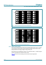
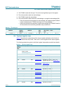
Table 25. I
2
C write cycle
Start TFA9812
Address
R/!W TFA9812 first
register address
MS
databyte
LS
databyte
More
data...
Stop
S 11010A
2
A
1
0 A ADDR A MS1 A LS1 <....> P