


TFA9812_2 © NXP B.V. 2009. All rights reserved.
Preliminary data sheet Rev. 02 — 22 January 2009 48 of 66
NXP Semiconductors
TFA9812
BTL stereo Class-D audio amplifier with I
2
S input
[1] R
s
is the series resistance of inductor of low-pass LC filter in the application.
[2] Output power measured across the loudspeaker load. This is based on indirect measurement of R
DSon
.
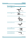
13.3 Timing
t
PD
propagation delay f
s
=
8 kHz - 3.6 - ms
11.025 kHz - 2.58 - ms
12 kHz - 2.39 - ms
16 kHz - 1.78 - ms
22.05 kHz - 1.3 - ms
24 kHz - 1.18 - ms
32 kHz - 892 - µs
44.1 kHz - 664 - µs
48 kHz - 600 - µs
64 kHz - 458 - µs
88.2 kHz - 320 - µs
96 kHz - 306 - µs
128 kHz - 67.2 - µs
176.4 kHz - 48 - µs
192 kHz - 40.8 - µs
PWM output
t
r
rise time I
O
= 0 A - 10 - ns
t
f
fall time I
O
= 0 A - 10 - ns
t
w(min)
minimum pulse width I
O
= 0 A - 40 - ns
R
DSon
drain-source on-state resistance per output MOSFET, for low and high
side
- 0.28 0.35 Ω
δ
max
maximum duty factor - - 0.96 -
Table 56. AC characteristics
…continued
Unless specified otherwise, V
DDA
=V
DDP
= 12 V, V
DDA(3V3)
=V
DDD(3V3)
= 3.3 V, T
amb
=25
°
C, R
s
< 0.1
Ω
[1]
, R
L
=8
Ω
,
f
i
= 1 kHz, f
s
= 44.1 kHz, f
sw
= 400 kHz, 24-bit I
2
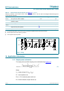
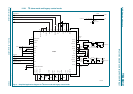
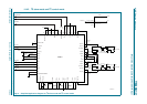
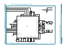
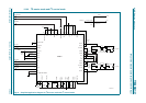
S input data, MCLK clock mode, typical application diagram (Figure 13).
Symbol Parameter Condition Min. Typ. Max. Unit
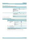
Table 57. Characteristics I
2
C bus interface; see Figure 10
V
DDD(3V3)
=V
DDA(3V3)
= 2.7 V to 3.6 V; V
DDA
=V
DDP
= 8 V to 20 V;T
amb
=
−
20
°
C to +85
°
C; all voltages referenced to ground;
unless otherwise specified.
Symbol Parameter Conditions Min Typ Max Unit
f
SCL
SCL clock frequency - - 400 kHz
t
LOW
LOW period of the SCL clock 1.3 - - µs
t
HIGH
HIGH period of the SCL clock 0.6 - - µs
t
r
rise time SDA and SCL signals
[1]
20 + 0.1 C
b
-- ns
t
f
fall time SDA and SCL signals
[1]
20 + 0.1 C
b
-- ns
t
HD;STA
hold time (repeated) START
condition
[2]
0.6 - - µs
t
SU;STA
set-up time for a repeated START
condition
0.6 - - µs