


TFA9812_2 © NXP B.V. 2009. All rights reserved.
Preliminary data sheet Rev. 02 — 22 January 2009 29 of 66
NXP Semiconductors
TFA9812
BTL stereo Class-D audio amplifier with I
2
S input
9. The TFA9812 sends the first byte. This is the most significant byte of the register.
10. The microcontroller asserts an acknowledge.
11. The TFA9812 sends the second byte.
12. The microcontroller asserts either an acknowledge or a negative acknowledge (NA).
– If the microcontroller has asserted an acknowledge, the targeted register address
is auto-increased by the TFA9812 and steps 9 to 12 are repeated.
– If the microcontroller has asserted a negative acknowledge, the TFA9812 frees the
I
2
C bus and the microcontroller generates a stop condition (P).
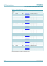
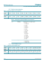
9.5 Top-level register map
Table 27 describes the assignments of the various register addresses to the functional
control or status areas at top level. There are 47 control registers and 2 status registers.
The following subsections give the individual register interpretations and bit level details.
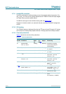
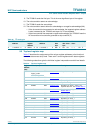
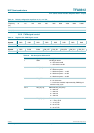
Table 26. I
2
C read cycle
Start TFA9812
address
R/!W First
register
address
TFA9812
address
R/!W MS
data
byte
LS
data
byte
More
data...
More
data...
Stop
S 11010A
2
A
1
0 A ADDR A Sr 11010A
2
A
1
1 A MS1 A LS1 <A> <....> NA P
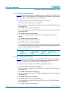
Table 27. Top-level register map
Register
address
(hex)
Default (hex) Access See: Description
0x00 0x0020;
Legacy_mode
R/W
Section 9.5.1 Interpolator settings and soft mute
0x0021; I
2
C_mode
0x01 0x0000 R/W
Section 9.5.2 Volume control
0x02 0x0006 R/W
Section 9.5.3 Format digital in
0x03 0x0002 R/W
Section 9.5.4 Equalizer configuration
0x04 0x0058 R/W
Section 9.5.5 Equalizer_A1 word_1; word_1 for
equalizer band A1, see
Section 8.5.1.2
0x05 0x4F40 R/W
Section 9.5.5 Equalizer_A1 word_2; see
Section 8.5.1.2
0x06 0x0058 R/W
Section 9.5.5 Equalizer_B1 word_1
0x07 0x4F40 R/W
Section 9.5.5 Equalizer_B1 word_2
0x08 0x0A63 R/W
Section 9.5.5 Equalizer_C1 word_1
0x09 0x4240 R/W
Section 9.5.5 Equalizer_C1 word_2
0x0A 0x0A63 R/W
Section 9.5.5 Equalizer_D1 word_1
0x0B 0x4240 R/W
Section 9.5.5 Equalizer_D1 word_2
0x0C 0x00B7 R/W
Section 9.5.5 Equalizer_A2 word_1
0x0D 0x4E40 R/W
Section 9.5.5 Equalizer_A2 word_2
0x0E 0x00B7 R/W
Section 9.5.5 Equalizer_B2 word_1
0x0F 0x4E40 R/W
Section 9.5.5 Equalizer_B2 word_2
0x10 0x14A2 R/W
Section 9.5.5 Equalizer_C2 word_1