


TFA9812_2 © NXP B.V. 2009. All rights reserved.
Preliminary data sheet Rev. 02 — 22 January 2009 43 of 66
NXP Semiconductors
TFA9812
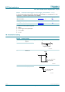
BTL stereo Class-D audio amplifier with I
2
S input
[1] V
ss
= V
SS1
= V
SS2
= REFA = REFD
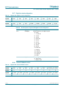
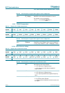
12. Thermal characteristics
[1] Measured in a JEDEC high K-factor test board (standard EIA/JESD 51-7).
[2] Measured in free air with natural convection.
[3] Strongly depends on where measurement is made on the case: worst-case value stated.
V
x
voltage on pin x DIAG
[1]
V
SS
− 0.3 V
SS
+ 12 V
POWERUP
[1]
V
SS
− 0.3 V
DDA
+ 0.3 V
ENABLE, GAIN, CSEL,
ADSEL2/PLIM2,
ADSEL2/PLIM1,SCL/SFOR,
SDA/MS, DATA, WS, BCK,
MCLK
[1]
V
SS
− 0.5 V
SS
+ 5.5 V
AVOL
[1]
V
SS
− 0.5 V
SS
+ 4.6 V
V
esd
electrostatic discharge voltage according to the human body model
STAB1 and STAB2 with
respect to other pins
−1750 +1750 V
all other pins −2+2 kV
according to the charge
device model
−500 +500 V
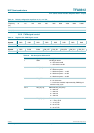
Table 53. Limiting values
…continued
In accordance with the Absolute Maximum Rating System (IEC 60134).
Symbol Parameter Conditions Min Max Unit
Table 54. Thermal Characteristics
Symbol Parameter Condition Min Typ Max Unit
R
th(j-a)
thermal resistance
from junction to
ambient
No air flow, JEDEC board
[1][2]
- - 42 K/W
No air flow; typical 4L board in
the NXP 4L reference
application
[2]
- - 36 K/W
No air flow; typical 2L board in
the NXP 2L reference
application
[2]
- - 42 K/W
R
th(j-c)
thermal resistance
from junction to case
[3]
5 - - K/W
R
th(j-lead)
thermal resistance
from junction to lead
Worst-case pin 5 - - K/W