


TFA9812_2 © NXP B.V. 2009. All rights reserved.
Preliminary data sheet Rev. 02 — 22 January 2009 27 of 66
NXP Semiconductors
TFA9812
BTL stereo Class-D audio amplifier with I
2
S input
[1] See, Section 9.5.10.
[2] Window Protection is only checked at power-up.
9. I
2
C bus interface and register settings
9.1 I
2
C bus interface
The TFA9812 supports the 400 kHz I
2
C bus microcontroller interface mode standard. This
can be used to control the TFA9812 and to exchange data with it when in I
2
C control
mode, see Section 8.2.1.
The TFA9812 can operate in I
2
C slave mode only as slave receiver or a slave transmitter.
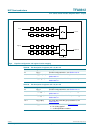
The serial hardware interface involves the pins of the TFA9812 as described in Table 22.
Voltage values applied to the I
2
C bus device address pins are interpreted as described in
Table 23.
9.2 I
2
C bus TFA9812 device addresses
Table 24 shows the register address options for the TFA9812 as part of the 8-bit byte that
contains the device address as well as the bit indicator read/write_not R/!W. The TFA9812
supports four different addresses, each of which can be configured using the pins
ADSEL1/PLIM1 and ADSEL2/PLIM2, see Table 22.
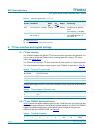
OFP PLL frequency > 140 MHz Floating OFP Floating Restart (fault to operating
when
PLL frequency < 140 MHz)
IBP BCK/WS is not 32 ± 2,
48 2 or 64 2
Floating - Floating Restart (fault to operating
when BCK/WS is 32 ± 2,
48 2 or 64 2)
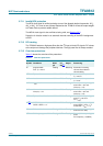
Table 21. Overview protections
…continued
Protections
Symbol Conditions DIAG
pin
I
2
C
flag
[1]
Output Recovering
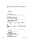
Table 22. I
2
C pins in I
2
C control mode
Pin name Description
SCL/SFOR I
2
C bus clock input
SDA/MS I
2
C bus data input and output
ADSEL2/PLIM2 I
2
C bus device address bit A2
ADSEL1/PLIM1 I
2
C bus device address bit A1
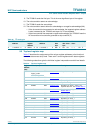
Table 23. I
2
C pin voltages in I
2
C control mode
Logic value Voltage A2/A1
0< V
IL
1> V
IH
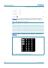
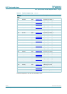
Table 24. I
2
C bus device address
(MSB) Bit (LSB)
11010A2A1R/!W