


TFA9812_2 © NXP B.V. 2009. All rights reserved.
Preliminary data sheet Rev. 02 — 22 January 2009 45 of 66
NXP Semiconductors
TFA9812
BTL stereo Class-D audio amplifier with I
2
S input
V
OH
HIGH-level output
voltage
At I
OH
= −0.4 mA V
DDD(3V3)
− 0.4 V - - V
V
OL
LOW-level output
voltage
At I
OL
= 4 mA - - 400 mV
C
L
load capacitance - - 50 pF
SDA/MS, SCL/SFOR pin
V
IH
HIGH-level input
voltage
With respect to V
SS2
0.7 × V
DDD(3V3)
- 5.5 V
V
IL
LOW-level input
voltage
With respect to V
SS2
−0.3 - 0.3 × V
DDD(3V3)
V
V
hys(i)
input hysteresis
voltage
With respect to V
SS2
0.1 × V
DDD(3V3)
-- V
C
i
input capacitance - - 2.5 pF
V
OL
LOW-level output
voltage
At I
OL
= 3 mA - - 400 mV
ENABLE, GAIN, CSEL, ADSEL2/PLIM2, ASEL1/PLIM1 pin
V
IH
HIGH-level input
voltage
With respect to V
SS2
0.7 × V
DDD(3V3)
-- V
V
IL
LOW-level input
voltage
With respect to V
SS2
- 0.3 × V
DDD(3V3)
V
V
hys(i)
input hysteresis
voltage
With respect to V
SS2
0.1 × V
DDD(3V3)
-- V
I
I
input current - 50 93 µA
Regulators
V
o
output voltage STAB1 − V
SS1
10 11 12 V
STAB2 − V
SS1
10 11 12 V
STABA − REFA 1.65 1.8 1.95 V
STABD − REFD 1.65 1.8 1.95 V
CDELAY pin
V
CDELAY
voltage on pin
CDELAY
Relative to positive
analog power supply
-V
DDA
−1- V
Crystal pins
V
o(xtal)(p-p)
peak-to-peak crystal
oscillator output
voltage
With respect to V
SS2
- 1.8 - V
AVOL pin
V
i
input voltage Mute level, with respect
to V
SS2
0.77 0.8 0.83 V
0 dB level with respect
to V
SS2
2.74 2.8 2.86 V
I
I
input current - - 1 µA
Table 55. DC characteristics
…continued
Unless specified otherwise, V
DDA
=V
DDP
= 12 V, V
SSP1
= V
SSP2
= 0 V, V
DDA(3V3)
=V
DDD(3V3)
= 3.3 V,
V
SS1
=V
SS2
= REFD = REFA = 0 V, T
amb
=25
°
C, R
L
=8
Ω
, f
i
= 1 kHz, f
s
= 44.1 kHz, f
sw
= 400 kHz, 24-bit I
2
S input data,
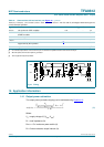
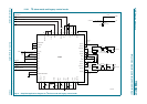
MCLK clock mode, typical application diagram (
Figure 13).
Symbol Parameter Condition Min Typ Max Unit