


TFA9812_2 © NXP B.V. 2009. All rights reserved.
Preliminary data sheet Rev. 02 — 22 January 2009 47 of 66
NXP Semiconductors
TFA9812
BTL stereo Class-D audio amplifier with I
2
S input
13.2 AC characteristics
Table 56. AC characteristics
Unless specified otherwise, V
DDA
=V
DDP
= 12 V, V
DDA(3V3)
=V
DDD(3V3)
= 3.3 V, T
amb
=25
°
C, R
s
< 0.1
Ω
[1]
, R
L
=8
Ω
,
f
i
= 1 kHz, f
s
= 44.1 kHz, f
sw
= 400 kHz, 24-bit I
2
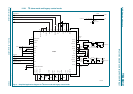
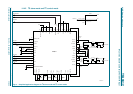
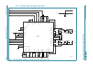
S input data, MCLK clock mode, typical application diagram (Figure 13).
Symbol Parameter Condition Min. Typ. Max. Unit
Output power per channel
P
o(RMS)
RMS output power Continuous time output power per channel; THD = 1 %, R
L
= 6 Ω
V
DDA
= V
DDP
= 12 V - 7.9 - W
V
DDA
= V
DDP
= 15 V - 12 - W
Continuous time output power per channel; THD = 10 %, R
L
= 6 Ω
V
DDA
= V
DDP
= 12 V - 9.7 - W
Short time (≤ 10 s) output power per channel; THD = 10 %, R
L
= 6 Ω
V
DDA
= V
DDP
= 15 V - 15 - W
Continuous time output power per channel; THD = 1 %, R
L
= 8 Ω
V
DDA
= V
DDP
= 12 V - 6.6 - W
V
DDA
= V
DDP
= 15 V - 10 - W
Continuous time output power per channel; THD = 10 %, R
L
= 8 Ω
V
DDA
= V
DDP
= 12 V - 8.3 - W
V
DDA
= V
DDP
= 13.5 V - 10 - W
V
DDA
= V
DDP
= 15 V - 12 - W
Short time (≤ 10 s) output power per channel; THD = 10 %, R
L
= 8 Ω
V
DDA
= V
DDP
= 17 V - 15 - W
Performance
THD+N total harmonic
distortion-plus-noise
P
O
= 1 W; AES17 brick wall filter - 0.07 0.1 %
S/N signal-to-noise ratio V
O
= 10 V; A-weighted - 103 - dB
V
n(o)
output noise voltage MCLK clock jitter < 200 ps; AES17 brick-wall filter
operating mode - 70 - µV
soft mute mode - 70 - µV
hard mute mode - 30 - µV
α
cs
channel separation P
o(RMS)
= 1 W; aggressor channel:
f
i
= 1 kHz
50 54 - dB
SVRR supply voltage ripple rejection V
ripple
= 2 V
pp
; f
ripple
= 100 Hz 55 60 - dB
η
po
output power efficiency R
L
= 8 Ω; P
o(RMS)
= 8.3 W
[2]
-88-%
R
L
= 6 Ω; P
o(RMS)
= 9.7 W
[2]
-83-%
Power-up times and delay times
t
d(on)
turn-on delay time - - 155 ms