


TFA9812_2 © NXP B.V. 2009. All rights reserved.
Preliminary data sheet Rev. 02 — 22 January 2009 22 of 66
NXP Semiconductors
TFA9812
BTL stereo Class-D audio amplifier with I
2
S input
The I
2
C controls for selecting the +24 dB gain can be found in Section 9.5.6. The GAIN
pin has no function In I
2
C mode.
The TFA9812 features also specific gain settings which are related to < 0.5 %, 10 %, 20 %
or 30 % clipping at the output of the TFA9812. These clipping values are only valid under
the following conditions:
• The volume control is set to 0 dB.
• The gain boost is set to 0 dB.
• A 0 dBFs I
2
S input signal is obtained.
The I
2
C controls for selecting a specific clip level can be found in Section 9.5.6. In Legacy
mode the clip level is set to 10 %.
8.5.6 Output power limiter
Output power can be limited to three discrete levels with respect to the maximum power.
The maximum power output value is determined by the value of the high voltage supply.
Clipping levels (see Section 8.5.5) still apply to the maximum levels of reduced output
voltage swings.
In I
2
C control mode the same output power limiting levels can be selected, see
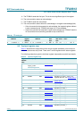
Section 9.5.6. In Legacy control mode two pins can be used to select the output power
limit level as shown in Table 18.
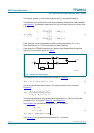
8.5.7 PWM control for performance improvement
The PWM switching frequency of the TFA9812 is dependent on:
• The sampling frequency, f
s
.
• The sampling frequency setting, f
s
(selected) (see Section 9.5.7).
• The PWM switching frequency setting, f
sw
(selected) (see Section 9.5.6).
Equation 9 shows the relationship between these settings and the PWM carrier
frequency:
(9)
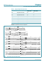
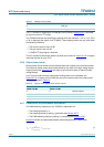
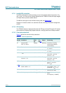
Table 17. GAIN pin functionality
GAIN pin value Function
0 0 dB gain
1 +24 dB gain
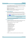
Table 18. Legacy mode output power limiter control
Pin value Function
ADSEL2/PLIM2 ADSEL1/PLIM1
0 0 Maximum power
0 1 Maximum power − 1.5 dB
1 0 Maximum power − 3.0 dB
1 1 Maximum power − 4.5 dB
f
sw
f
s
f
s selected)()
----------------------------
f
sw selected()
⋅=