


TFA9812_2 © NXP B.V. 2009. All rights reserved.
Preliminary data sheet Rev. 02 — 22 January 2009 6 of 66
NXP Semiconductors
TFA9812
BTL stereo Class-D audio amplifier with I
2
S input
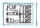
Figure 1 shows the block diagram of the TFA9812. For a detailed description of the audio
signal path see Section 8.1.
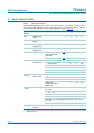
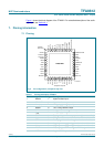
7. Pinning information
7.1 Pinning
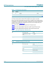
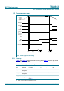
Fig 2. Pin configuration, transparent top view
Table 3. Pinning description TFA9812
Pin Symbol Type Description
1 XTALIN I Crystal oscillator input
2 XTALOUT O Crystal oscillator output
3V
DDA(3V3)
P Analog supply voltage (3.3 V)
4 STABA O 1.8 V analog stabilizer output
5 REFA P Analog reference voltage
6V
DDA
P Analog supply voltage (8 V to 20 V)
7 TEST1 I Test signal input 1. For test purposes only (connect to V
SS
)
8V
SS1
P PCB ground reference
9 STAB2 O Decoupling of internal 11 V regulator for channel 2 drivers
10 V
SSP2
P Negative power supply voltage for channel 1 and channel 2
11 V
SSP2
P Negative power supply voltage for channel 1 and channel 2
12 BOOT2N O Bootstrap high-side driver negative PWM output channel 2
13 OUT2N O Negative PWM output channel 2
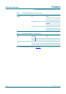
010aaa218
TFA9812HN
BOOT1N
V
SSP2
BOOT2N
V
SSP1
V
SSP2
V
SSP1
STAB2 STAB1
V
SS1
DIAG
TEST1 CDELAY
V
DDA
POWERUP
REFA AVOL
STABA ENABLE
V
DDA(3V3)
GAIN
XTALOUT CSEL
XTALIN ADSEL2/PLIM2
OUT2N
OUT2N
BOOT1P
OUT2P
OUT1P
V
DDP
V
DDP
OUT1P
OUT1P
BOOT1P
OUT1N
OUT1N
V
SS2
MCLK
BCK
WS
DATA
TEST2
REFD
STABD
V
DDD(3V3)
SDA/MS
SCL/SFOR
ADSEL1/PLIM1
12 25
11 26
10 27
9 28
8 29
7 30
6 31
5 32
4 33
3 34
2 35
1 36
13
14
15
16
17
18
19
20
21
22
23
24
48
47
46
45
44
43
42
41
40
39
38
37
terminal 1
index area
Transparent top view