


TFA9812_2 © NXP B.V. 2009. All rights reserved.
Preliminary data sheet Rev. 02 — 22 January 2009 25 of 66
NXP Semiconductors
TFA9812
BTL stereo Class-D audio amplifier with I
2
S input
8.7.6 Overdissipation protection
When the output current of the power amplifiers exceeds a current value of 3 A and the
temperature is above 140 °C, overdissipation protection is activated and the device enters
Sleep mode. A restart will be initiated automatically when the two overdissipation
conditions are both changed to ‘false’.
Overdissipation is flagged by a low DIAG pin and by a high DIAG I
2
C status bit, see
Section 9.5.10.
Under normal conditions thermal foldback prevents overdissipation protection from being
triggered. I
2
C settings remain valid.
8.7.7 Window protection
Window protection is a feature for protecting the device against shorts from the outputs to
the ground or supply lines. If during power-up one of the outputs is shorted to V
SSPx
or
V
DDP
, power-up does not proceed any further. The trigger levels for these conditions are:
• OUTxx > V
DDA
− 1 V, or
• OUTxx < REFA + 1 V.
The WP alarm is flagged by a low DIAG pin and by a high DIAG I
2
C status bit, see
Section 9.5.10.
8.7.8 Lock protection
When the selected clock input source (MCLK, BCK or crystal) stops running, the TFA9812
is able to detect this and set the output stages to 3-state mode. Without this protection
peripheral devices in an application might be damaged.
The PLL lock indication is an I
2
C reading and will be ‘false’ in the event of a clock
interruption, see Section 9.5.10.
8.7.9 Underfrequency protection
UFP sets the output stages to 3-state mode when the clock input source is too low. The
PWM switching frequency can becomes critically low when the clock input source is lower
than specified. Without UFP peripheral devices in an application might be damaged.
The status of the UFP is shown in I
2
C reading register, see Section 9.5.10.
8.7.10 Overfrequency protection
OFP sets the output stages to 3-state mode when the clock input source is too high. The
PWM controller can become unstable when the clock input source is higher than
specified. Without OFP peripheral devices in an application might be damaged.
The status of the OFP is shown in I
2
C reading register, see Section 9.5.10.
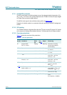
Table 20. Undervoltage trigger levels
Pin name UVP level DIAG pin (protection active)
Min Max
V
DDA
≥ 7 V < 8 V LOW
V
DDA(3V3)
≥ 1.6 V < 3 V -