


TFA9812_2 © NXP B.V. 2009. All rights reserved.
Preliminary data sheet Rev. 02 — 22 January 2009 23 of 66
NXP Semiconductors
TFA9812
BTL stereo Class-D audio amplifier with I
2
S input
The selected PWM switching frequency is 400 kHz by default and can be set to 350 kHz,
700 kHz and 750 kHz in I
2
C control mode. In Legacy mode 400 kHz is the only option and
this scales linearly if 32 kHz or 48 kHz is used as f
s
.
Remark: The selected sample frequency, f
s
(selected) must be equal to the sample
frequency (f
s
) in I
2
C control mode.
Remark: The performance of AM radio reception can sometimes be improved by
selecting non-interfering frequencies for the PWM signal.
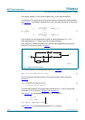
8.6 Class-D amplification
The Class-D power amplification of the PWM signal is carried out in two BTL power
stages. The output signal voltage level is determined by the values on the V
DDP
pins.
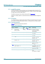
The power amplifiers can be explicitly put into 3-state mode by using the pin ENABLE as
shown in Table 19. The ENABLE pin is functional in Legacy mode and in I
2
C mode.
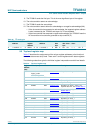
[1] Can be overruled by a forced 3-state in Sleep or Fault mode.
8.7 Protection mechanisms
The TFA9812 has a wide range of protection mechanisms to facilitate optimal and safe
application. All of these are active in both I
2
C and Legacy control modes.
The following protections are included in the TFA9812:
• Thermal Foldback (TF)
• OverTemperature Protection (OTP)
• OverCurrent Protection (OCP)
• OverVoltage Protection (OVP)
• UnderVoltage Protection (UVP)
• Window Protection (WP)
• Lock Protection (LP)
• UnderFrequency Protection (UFP)
• OverFrequency Protection (OFP)
• Invalid BCK Protection (IBP)
• DC-blocking
• ESD
The reaction of the device to the different fault conditions differs per protection.
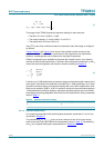
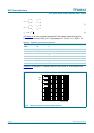
Table 19. ENABLE pin functionality
ENABLE pin value Function
0 Output stages in 3-state mode.
1 Switching enabled
[1]
.