


VHF (7610) CIRCUIT DESCRIPTION
5A-5
November 1998
Part No. 001-7600-001
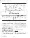
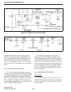
The phase detector determines the phase differ-
ence between these signals and then produces output
pulses on pin 8 which are filtered by the loop filter.
This filter consists of R43-R45, C60, and C61. The
output of this filter is the DC control voltage applied to
the VCO. The phase detector increases or decreases
this control voltage to change the VCO frequency.
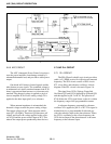
5.3.2 VCO CIRCUIT
The VCO signal is amplified by buffer amplifiers
Q6 and Q4 and is then applied to T/R switch D5 and
D6. The VCO receive injection signal is applied to
first mixer Q13 via bandpass filter L23, L24, and
C116-C118. Likewise, the VCO transmit signal is
applied to driver Q1 via buffer amplifiers Q2 and Q3.
Part of the Q6 output signal is fed back to PLL IC2 as
described in the preceding section.
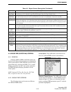
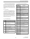
5.4 VHF IC PIN DESCRIPTIONS
5.4.1 VHF POWER SUPPLY
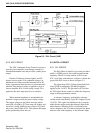
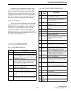
5.4.2 VHF CPU IC1 PORT ALLOCATION
Line Description
VCC Unswitched input voltage to the transceiver.
HV VCC supply voltage switched by Q25 and Q26.
When the [POWER] switch is pressed, the CPU
outputs the “PWON” control signal to this circuit
to turn the HV supply on.
CPU5V Common 5V supply for the CPU produced from
the VCC supply by CPU5V regulator IC9. The
circuit outputs this voltage regardless of the
transceiver on-off condition.
8V Common 8V supply produced from the HV
supply by 8V regulator Q36.
5V Common 5V supply produced from the VCC
supply by 5V regulator Q29/Q30.
R5 Receive 5V supply produced by R5 regulator
Q27 using the “T5C” signal from I/O expander
IC IC11.
T5 Transmit 5V supply controlled by T5 regulator
Q28 using the “T5C” signal from I/O expander
IC11.
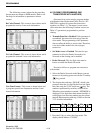
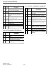
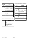
Pin
No.
Port
Name
Description
1 VIN Input port for overvoltage detection from
the vehicle power source.
12 SCK Outputs clock signal to EEPROM IC3,
PLL IC2 (main unit) and expanders IC5,
IC11 (main unit), etc.
13 SI Input port for the data signal from
EEPROM IC3, etc.
14 SO Outputs data signal to EEPROM IC3, PLL
IC2 (main unit) and expanders IC5, IC11
(main unit).
16 CLIN Input port for cloning signal.
17 CLOUT Output port for cloning signal.
18 POSW Input for the POWER switch. Low =
POWER switch pushed.
19 NOIS NOIS signal input port from the FM IF
IC3 (main unit) for noise squelch
operation.
26 PTT Input port for the PTT switch. Low = PTT
switch pushed.
32 RFATT Outputs RF attenuator control signal to the
attenuator switch (Q35 on main unit).
Low = Attenuator function on.
36 UNLK Input port for PLL unlock signal from the
PLL IC2 (main unit). High = unlock.
37 PWON Outputs control signal for the power
switching circuit (Q25 on main unit) and
5V regulator Q29, Q30 (main unit).
38 DIM Outputs control signal for LCD backlight.
Low = LCD backlight on.
39 EXTPTT Input port for the PTT switch from exter-
nal connector J3 (main unit). Low = Exter-
nal PTT switch on.
40 DIM Input port for the LCD backlight control
signal from external connector J3 (main
unit). Low = External dimmer switch on.
41 PLST Outputs strobe signals for PLL IC2 (main
unit).
42 DAST Outputs strobe signals for level controller
IC5 (main unit).
43 EXST Outputs strobe signals for the I/O
expander IC11 (main unit).
45,
46
KS1,
KS2
Output ports for the key matrix.
47-
50
KR3-
KR10
Input ports for the key matrix.