


5A-1
November 1998
Part No. 001-7600-001
VHF (7610) CIRCUIT DESCRIPTION
NOTE: A VHF transceiver block diagram is located
on page 8-1.
5.1 VHF RECEIVER CIRCUIT
5.1.1 ANTENNA SWITCHING CIRCUIT
The antenna switching circuit functions as a low-
pass filter while receiving and a resonator circuit while
transmitting. This prevents the transmit signal from
entering the receiver in the transmit mode.
Received signals enter the antenna connector and
pass through a low-pass filter consisting of L1-L3, C1-
C3, C8-C10, and C11-C13. The filtered signal is then
fed through a quarter-wave type antenna switching cir-
cuit formed by D13, D14, and L13 and applied to the
receiver RF circuit.
5.1.2 RF CIRCUIT
The RF circuit amplifies the frequencies that are
within the receive band range and attenuates out-of-
band signals.
The signal from the antenna switching circuit
passes through attenuator D13/D14. The attenuator
circuit functions only when the attenuator function is
assigned to a programmable key. It is enabled to mini-
mize RF amplifier distortion caused by excessively
strong receive signals.
When the attenuator function is turned on, CPU
IC1, pin 32 switches the voltage level of the “RF
ATT” line from high to low and then controls the
attenuator switch Q35. The D13/D14 current then
increases and D13/D14 act as an attenuator.
This signal is then applied to a two-stage tunable
bandpass filter controlled by D16 and D17. The fil-
tered signals are amplified by RF amplifier Q12 and
applied to another two-stage bandpass filter controlled
by D18-D21. These filters attenuate unwanted signals.
The filtered signal is then applied to the first mixer
Q13.
The tunable bandpass filters controlled by D16-
D21 employ varactor diodes to tune them to the center
frequency of the RF passband. This gives a wide band-
width receiver good image response rejection. The
diodes are controlled by the CPU IC1 via level
controller IC5.
5.1.3 FIRST MIXER AND FIRST IF CIRCUITS
The first mixer circuit converts the received sig-
nal to a fixed frequency first IF signal of 31.050 MHz.
The RF signal from the bandpass filter is applied to the
first mixer Q13. This signal is mixed with the first LO
signal from VCO Q7/Q8 and buffers Q6-Q4 to pro-
duce the IF signal.
The 31.050 MHz first IF signal then passes
through a pair of crystal filters (FI1A/B) which sup-
press out-of-band signals. The filtered signal is then
amplified by first IF amplifier Q14 and applied to sec-
ond IF circuit IC3.
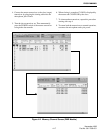
5.1.4 SECOND IF AND DEMODULATOR
CIRCUITS
The second mixer circuit converts the 31.050
MHz first IF signal to a 450 kHz second IF signal. A
double-conversion superheterodyne receiver like this
improves the image rejection ratio and provides a
stable receiver gain.
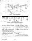
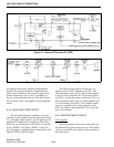
FM IF system IC3 contains second mixer, limiter
amplifier, quadrature detector, active filter and noise
amplifier circuits (see Figure 5-1). The first IF signal
from IF amplifier Q14 is applied to IC3, pin 16 which
is the input to the second mixer section. The 31.050
MHz first IF signal is mixed with the 30.600 MHz sec-
ond LO signal to produce the 450 kHz second IF sig-
nal. The PLL reference frequency of 15.300 MHz is
doubled to produce the 30.600 MHz second LO signal.
The second IF signal is fed out of IC3 on pin 3
and applied to ceramic filters FI3 and FI4 with narrow
band operation or only FI4 with wideband operation
(bypassing FI3). It is then fed back into IC3 on pin 5
and applied to the limiter amplifier and quadrature
detector. The quadrature detector demodulates the
audio signal contained in the second IF signal. Com-
ponents connected to pins 10 and 11 including X3
SECTION 5A VHF (7610) CIRCUIT DESCRIPTION