


VHF (7610) CIRCUIT DESCRIPTION
5A-3
November 1998
Part No. 001-7600-001
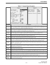
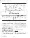
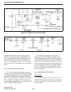
Part of the AF signal from pin 9 of FM IF circuit
IC3 is applied to pin 24 of level controller IC5. This
device allows the CPU to control the squelch threshold
level. The level-controlled output signal on pin 23 is
applied to IC3, pin 8 which is the input of an internal
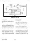
filter (see Figure 5-1). Noise frequencies of about 10
kHz are passed and then fed out on pin 7 and also
applied to an internal noise detector.
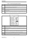
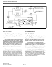
The detected noise signal is rectified and fed out
on pin 13 without smoothing. The noise signal (NOIS)
is then applied to pin 19 of CPU IC1. The CPU ana-
lyzes the noise condition and outputs the RMUT sig-
nal via I/O expander IC11. This signal controls AF
mute switches IC4a and c (see Figure 5-2).
Call Guard (CTCSS/DTCS) Operation
The tone Call Guard squelch circuit detects AF
signals and opens the squelch only when receiving a
signal containing a matching subaudible tone or code
(CTCSS or DTCS). When tone squelch is in use and a
signal with a mismatched or no subaudible tone is
received, the tone squelch circuit mutes the AF signals
even when noise squelch is open.
A portion of the audio signal from amplifier IC7a
passes through low-pass filter Q5 in the front unit to
remove voice signals. It is then applied to CPU IC1 on
pin 97 via the “CTCIN” line. The CPU detects the
CTCSS or DTCS signaling and controls the AF mute
switch via I/O expander IC11.
5.2 VHF TRANSMITTER CIRCUIT
5.2.1 MICROPHONE AMPLIFIER CIRCUIT
The microphone amplifier circuit amplifies the
microphone audio signal to the level required by the
modulation circuit and also provides pre-emphasis.
The microphone audio signal is amplified by
IC7d, with R172 and C295 on the output providing
pre-emphasis. The microphone audio signal is then fed
to switch IC4 on pin 4 and the switched output signal
is on pin 3. This signal is then applied to high-pass fil-
ter IC8a/b which attenuates frequencies in the Call
Guard (CTCSS/DTCS) range. This is the same filter
used for receive audio filtering.
The signal is then fed to IC7b and IC7c which
provide buffering and amplification. Deviation limit-
ing is then provided by level controller IC5. The input
to this device is pin 16 and the output is pin 15. The
signal is then fed to splatter filter IC6b and switch IC4.
The input is on pin 11 and the output is on pin 10. The
modulation signal is then applied to the PLL circuit as
“MOD”.
Narrow band/wideband switch Q21 is connected
to the input of the splatter filter IC6b and switched by
the “NWC” signal from the I/O expander IC11. When
“NWC” is high, Q21 shifts the filter cut-off frequency
for narrow band deviation selection.
5.2.2 MODULATION CIRCUIT
The microphone audio signal modulates the fre-
quency of VCO Q7/Q8. The “MOD” signal from
switch IC4, pin 10 changes the reactance of diode D9
which frequency modulates the VCO frequency. The
modulated VCO signal is amplified by buffer amplifi-
ers Q6, Q5, and Q4 and applied to the transmit driver
circuit.
5.2.3 TRANSMIT DRIVER CIRCUIT
The transmit driver circuit amplifies the VCO
oscillating signal to the level required by the power
amplifier module. The RF signal from buffer amplifier
Q4 passes through the T/R switch D5 and is amplified
by the buffer-amplifiers Q3 and Q2 and driver Q1. The
signal is then applied to the power amplifier module
IC1.
5.2.4 POWER AMPLIFIER MODULE
The power amplifier module amplifies the driver
signal to the output power level. The RF signal from
the driver Q1 is applied to the power module which
produces 45 watts of output power at the antenna jack.
The amplified signal is fed through antenna
switching circuit D3 and D4, a low-pass filter and
APC detector, and is then applied to the antenna jack.
The collector voltage of driver Q1 and the control
voltage on pin 2 of the power module IC1 come from
APC transistors Q17 and Q18. Transmit switch Q23
turns off Q17 and Q18 when the transmitter is
disabled.