


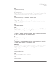

q
DSP Command Register: This register is used to assert VXI interrupts and toggle
various status register bits. Many of the bits in this register are grouped into related
Clock and Value pairs. This allow the bits to be modified independently with single
register writes. In order to change an output value, the Clock bit must be written as a
one (1), while the Value is written as the desired output value. Writing the Clock bit as
a zero (0) will not change the output state. The current state is read from the Value bit.
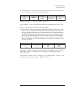
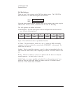
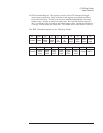
The DSP Command register has the following format:
Bit 31-24 23 22 21 20 19 18 17 16
Contents Unused
FIFO
Enable
Clock
FIFO
Enable
Value
FIFO
In
Clock
FIFO
In
Value
DONE
Clock
DONE
Value
ERRn
Clock
ERRn
Value
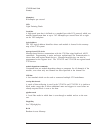
Bit 15 14 13 12 11 10 9-8 7-0
Contents
Q Resp
Ready
Clock
Q Resp
Ready
Value
Cmd
Ready
Clock
Cmd
Ready
Value
IRQ
Enable
Clock
IRQ
Enable
Value
Unused IRQ7-0
VT1433B User's Guide
Register Definitions
A-15