


q
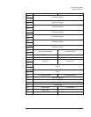
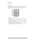
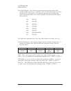
Control Register: A write to this register causes specific actions to be executed by the
device. The actions are described in the following table.
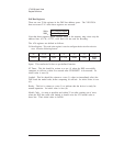
Bit 15 14-2 1 0
Contents
A24/A32
Enable
Unused Sysfail Inhibit Reset
A24/A32 Enable: A one (1) in this field enables access to the device’s A24
VME Bus registers. A zero (0) disables such access.
Sysfail Inhibit: A one (1) disables the device from driving the SYSFAIL* line.
Reset: A one (1) forces the device into a reset state.
q
Offset Register: This read/write register defines the base address of the device’s A24
registers. The four most significant bits of the Offset register are the values of the four
most significant bits of the device’s A24 register addresses. The 12 least significant
bits of the Offset register are always zero (0). Thus, the Offset register bits 15-12 map
the VME Bus address lines A23-A20 for A24 register accesses. A read of the Offset
register always returns the address offset most recently written to the Offset register.
q
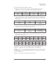
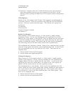
Port Control Register: This register is used to override the Local Bus control of the
device. (This applies to VT1433B modules that are equipped to use Local Bus). It has
the following format:
Bit 15-2 1 0
Contents Unused
LBus
Pipe
LBus
Enable
LBus Pipe: Writing a one (1) puts the Local Bus into pipeline mode, if the LBus
Enable bit is also set. Writing a zero (0) allows the Local Bus to operate in
some other mode.
LBus Enable: Writing a one (1) enables the Local Bus interface. Writing a zero
(0) disables the local bus interface. RESET VALUE: 0
VT1433B User's Guide
Register Definitions
A-7