


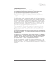
The VXI Bus Registers are defined as follows:
q
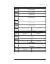
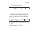
Id Register: A read of this 16 bit register provides information about the device’s
configuration. Its value is always CFFF16 as defined in the following table.
Bit 15-14 13-12 11-0
Contents
11
(Register Based Device)
00
(A16/A24)
111111111111
(Agilent’s ID)
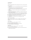
q
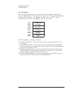
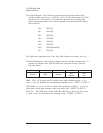
Logical Address Register: A write to this register changes the device’s logical address
according to the VXI Bus Dynamic Configuration protocol. Its format is defined in the
following table.
Bit 15-8 7-0
Contents No effect
Logical
Address
q
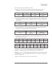
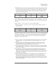
Device Type Register: A read of this register provides information about the device’s
configuration. Its format is defined in the following table.
Bit 15-12 11-0
Contents
0011
(1MB of A24)
Model Code
(202
16 for VT1433B)
q
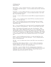
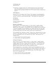
Status Register: A read of this register provides information about the device’s status as
defined in the following table.
Bit 15 14 13-12 11 10 9 8
Contents
A24
Active
MODID* Unused
Block
Ready
Data
Ready
ST
Done
Loaded
Bit 76543210
Contents Done Err* Unused
HW
OK
Ready Passed
Q Resp
Ready
Cmd
Ready
A24 Active: A one (1) in this field indicates that the A24 registers can be
accessed. It reflects the state of the Control register’s A24 Enable bit.
MODID*: A one (1) in this field indicates that the device is not selected via the
P2 MODID line. A zero (0) indicates that the device is selected by a high state
on the P2 MODID line.
Unused: A read of these bits will always return zero (0).
VT1433B User's Guide
Register Definitions
A-5