


The A24 Registers
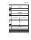
The following A24 registers are accessible at the base address defined by the
device’s offset Register. The registers at offsets 0 to E
16
are not accessible using
longword (D32) accesses. The registers at offsets 10
16
to FFFFF
16
may be
accessed by any of the of the D08(EO), D16 or D32 modes.
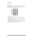
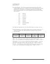
FFFFF16
8000 016
Movable DSP
Bus Window
7FFFF16
3000 016
Fixed DSP
Bus Window
2FFFF16
2000 016
Send/Receive
Data Registers
1FFFF16
0004 F16
Fixed DSP
Bus Window
0003 F16
0000 016
VXI Bus A16
Registers
The A24 registers are defined as follows:
q
VXI Bus A16 Registers: These are the same registers accessed at the device’s A16
base address.
q
Fixed DSP Bus Window: Accesses to this region are mapped to the corresponding
locations at the base of the internal DSP’s memory map, also accessible through Page 0
of the moveable DSP bus window.
q
Send/Receive Data Registers: Accesses to any address in this region will read/write
the Send and Receive Data registers defined in the A16 register set. VME Bus D32
Block Transfers are supported for these addresses only.
q
Movable DSP Bus Window: Accesses to this region are mapped (by the Page Map
register) to different 512 kB regions of the internal DSP bus.
VT1433B User's Guide
Register Definitions
A-4