


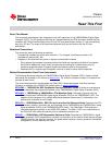
Wait
state
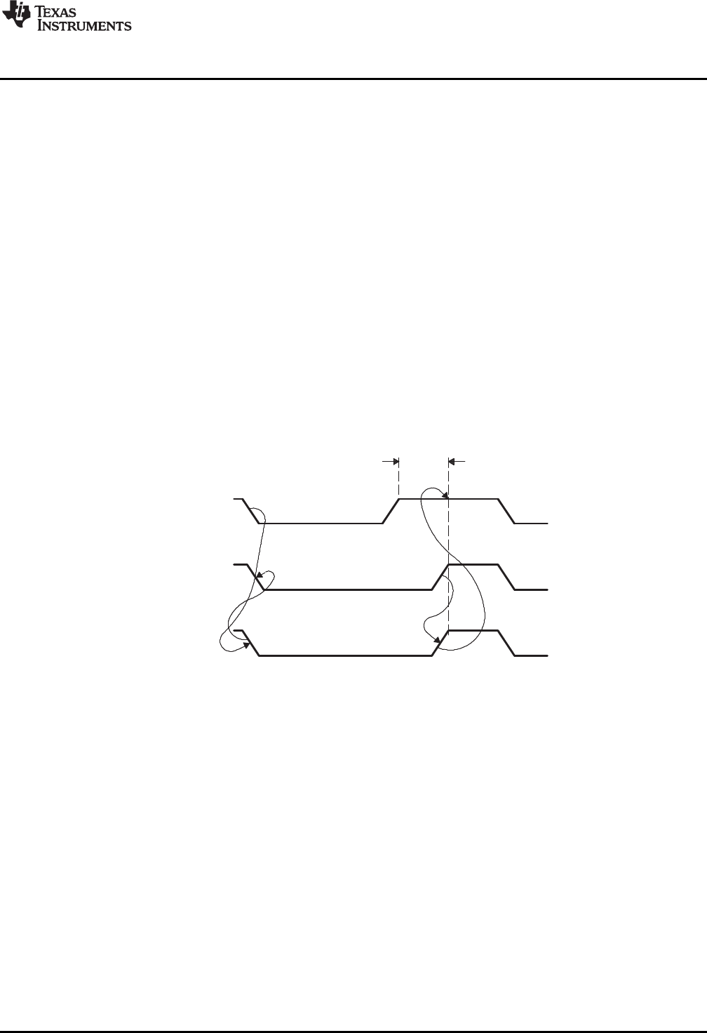
Start HIGH
period
SCL from
device #1
SCL from
device #2
Bus line
SCL
www.ti.com
Peripheral Architecture
The prescaler (IPSC bit in ICPSC) must only be initialized while the I2C module is in the reset state
(IRS = 0 in ICMDR). The prescaled frequency only takes effect when the IRS bit in ICMDR is changed to
1. Changing the IPSC bit in ICPSC while IRS = 1 in ICMDR has no effect. Likewise, you must configure
the I2C clock dividers (ICCH bit in ICCLKH and ICCL bit in ICCLKL) while the I2C module is still in reset
(IRS = 0 in ICMDR).
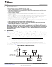
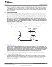
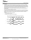
2.3 Clock Synchronization
Only one master device generates the clock signal (SCL) under normal conditions. However, there are
two or more masters during the arbitration procedure; and, you must synchronize the clock so that you
can compare the data output. Figure 4 illustrates the clock synchronization. The wired-AND property of
SCL means that a device that first generates a low period on SCL (device #1) overrules the other devices.
At this high-to-low transition, the clock generators of the other devices are forced to start their own low
period. The SCL is held low by the device with the longest low period. The other devices that finish their
low periods must wait for SCL to be released before starting their high periods. A synchronized signal on
SCL is obtained, where the slowest device determines the length of the low period and the fastest device
determines the length of the high period.
If a device pulls down the clock line for a longer time, the result is that all clock generators must enter the
wait state. This way, a slave slows down a fast master and the slow device creates enough time to store a
received data word or to prepare a data word that you are going to transmit.
Figure 4. Synchronization of Two I2C Clock Generators During Arbitration
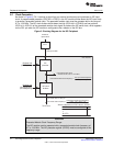
2.4 Signal Descriptions
The I2C peripheral has a serial data pin (SDA) and a serial clock pin (SCL) for data communication, as
shown in Figure 1. These two pins carry information between the C642x device and other devices that are
connected to the I2C-bus. The SDA and SCL pins both are bi-directional. They each must be connected to
a positive supply voltage using a pull-up resistor. When the bus is free, both pins are high. The driver of
these two pins has an open-drain configuration to perform the required wired-AND function.
See the device-specific data manual for additional timing and electrical specifications for these pins.
2.4.1 Input and Output Voltage Levels
The master device generates one clock pulse for each data bit that is transferred. Due to a variety of
different technology devices that can be connected to the I2C-bus, the levels of logic 0 (low) and logic 1
(high) are not fixed and depend on the associated power supply level. See the device-specific data
manual for more information.
11
SPRUEN0D–March 2011 Inter-Integrated Circuit (I2C) Peripheral
Submit Documentation Feedback
© 2011, Texas Instruments Incorporated