


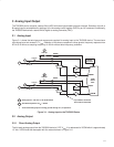
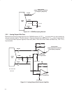
1−5
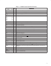
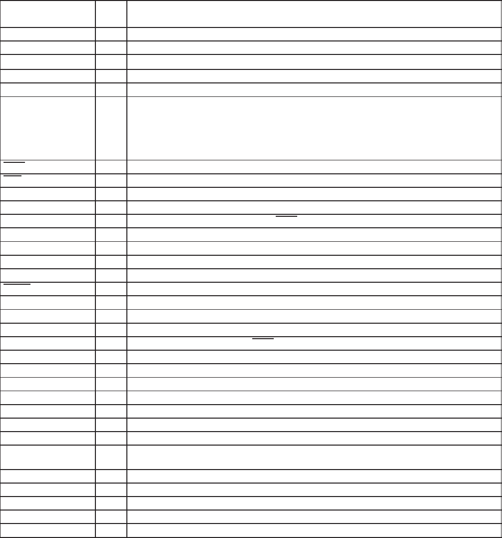
Table 1−1. TAS3002 Terminal Functions (Continued)
TERMINAL
I/O
DESCRIPTION
NAME NO.
I/O
DESCRIPTION
CAP_PLL 10 I Loop filter for internal phase-locked loop (PLL)
CLKSEL 11 I Logic low selects 256f
S
; logic high selects 512f
S
MCLK
CS1 7 I I
2
C address bit A0; low = 68h, high = 6Ah
DV
DD
17 I Digital power supply (3.3 V)
DV
SS
18 I Digital ground
GPI0
GPI1
GPI2
GPI3
GPI4
GPI5
28
29
30
31
32
33
I Switch input terminals
IFM/S 21 I Digital audio I/O control (low = input; high = output)
INPA 5 O Low when analog input A is selected (will sink 4 mA)
LINA 1 I Left channel analog input 1
LINB 48 I Left channel analog input 2
LRCLK/O 19 I/O Left/right clock input/output (output when IFM/S is high)
MCLKO 12 O MCLK output for slave devices
NC 34 No connection; Can be used as a printed circuit board routing channel
NC 36 No connection; Can be used as a printed circuit board routing channel
PWR_DN 8 I Logic high places the TAS3002 device in power-down mode
RESET 6 I Logic low resets the TAS3002 device to the initial state
RINA 40 I Right channel analog input 1
RINB 41 I Right channel analog input 2
SCL 15 I/O I
2
C clock connection
SCLK/O 20 I/O Shift (bit) clock input (output when IFM/S is high)
SDA 16 I/O I
2
C data connection
SDIN1 22 I Serial data input 1
SDIN2 23 I Serial data input 2
SDOUT0 25 O Serial data output from ADC
SDOUT1 26 O Serial data output (from internal audio processing)
SDOUT2 24 O Serial data output (a monaural mix of left and right, before processing)
TEST 9 I Reserved manufacturing test terminal; connect to DV
SS
VCOM 38 O Digital-to-analog converter mid-rail supply (decouple with parallel combination of 10-µF and 0.1-µF
capacitors)
V
REFM
45 I ADC minus voltage reference
V
REFP
44 I ADC plus voltage reference
V
RFILT
2 O Voltage reference low pass filter
XTALI/MCLK 13 I Crystal or external MCLK input
XTALO 14 I Crystal input (crystal is connected between terminals 13 and 14)