


6−1
6I
2
C Serial Control Interface
6.1 Introduction
Control parameters for the TAS3002 device can be loaded from an I
2
C serial EEPROM by using the TAS3002 master
interface mode. If no EEPROM is found, the TAS3002 device becomes a slave device and loads from another I
2
C
master interface. Information loaded into the TAS3002 registers is defined in Appendix A.
The I
2
C bus uses terminals 16 (SDA for data) and 15 (SCL for clock) to communicate between integrated circuits in
a system. These devices can be addressed by sending a unique 7-bit slave address plus R/W
bit (1 byte). All
compatible devices share the same terminals via a bidirectional bus using a wired-AND connection. An external
pullup resistor must be used to set the high level on the bus. The TAS3002 device operates in standard mode up to
100 kbps with as many devices on the bus as desired up to the capacitance load limit of 400 pF.
Furthermore, the TAS3002 device supports a subset of the SMBus protocol. When it is attached to the SMBus, then
byte, word, and block transfers are supported. The SMBus NAK function is not supported and care must be taken
with the sequence of the instructions sent to the TAS3002 device.
Additionally, the TAS3002 device operates in either master or slave mode; therefore, at least one device connected
to the I
2
C bus must operate in master mode.
6.2 I
2
C Protocol
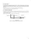
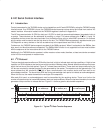
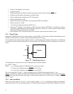
The bus standard uses transitions on SDA while the clock is high to indicate start and stop conditions. A high-to-low
transition on SDA indicates a start and a low-to-high transition indicates a stop. Normal data bit transitions must occur
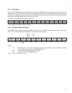
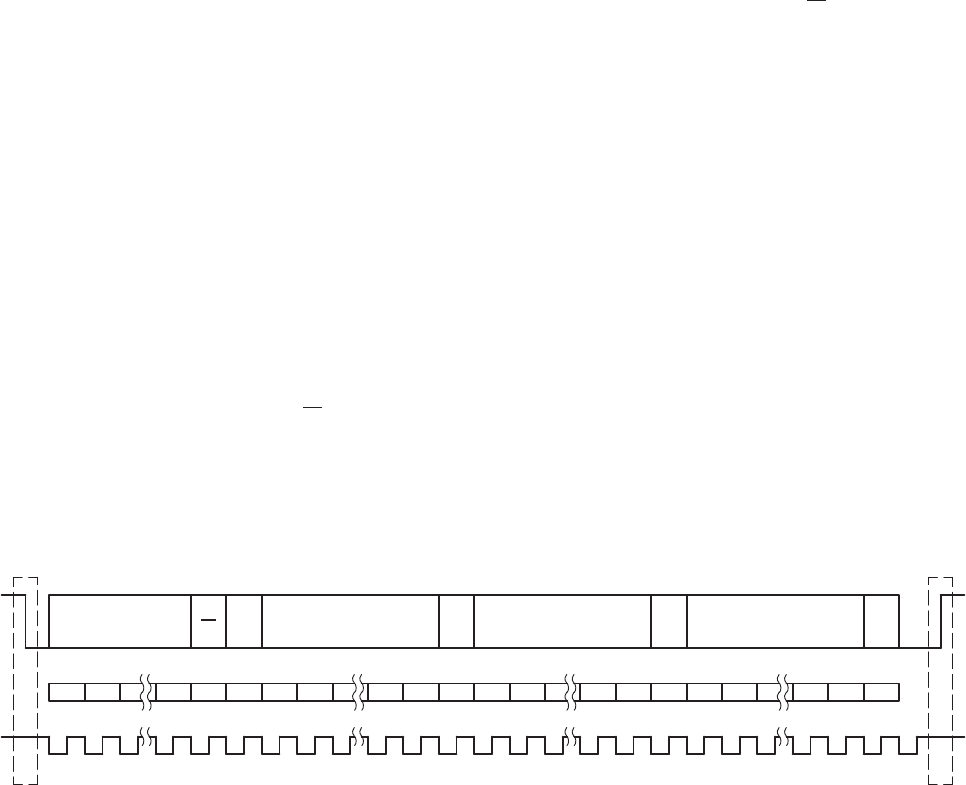
within the low time of the clock period. Figure 6−1 shows these conditions. These start and stop conditions for the
I
2
C bus are required by standard protocol to be generated by the master. The master must also generate the 7-bit
slave address and the read/write (R/W
) bit to open communication with another device and then wait for an
acknowledge condition. The slave holds SDA low during acknowledge clock period to indicate an acknowledgment.
When this occurs, the master transmits the next byte of the sequence.
After each 8-bit word, an acknowledgment must be transmitted by the receiving device. There is no limit on the
number of bytes that can be transmitted between start and stop conditions. When the last word transfers, the master
generates a stop condition to release the bus. Figure 6−1 shows a generic data transfer sequence.
8-Bit Register Data
for Address (N+2)
SCL
SDA
Start
0
A
167
8-Bit Register Data
for Address (N+1)
0
A
167
8-Bit Register Data
for Address (N)
0
A
167
7-Bit
Slave Address
0
A
167
R/
W
Stop
Figure 6−1. Typical I
2
C Data Transfer Sequence