


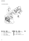
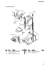
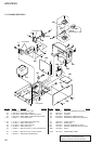
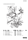
90
HCD-PX333
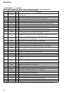
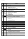
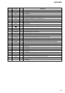
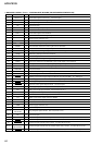
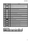
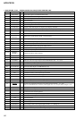
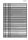
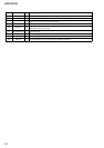
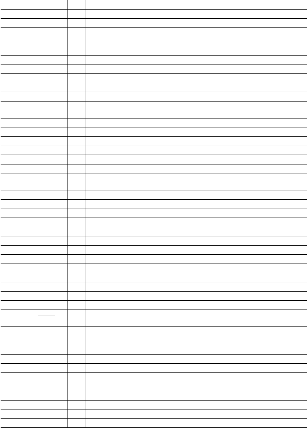
• MAIN BOARD IC501 µPDSS3033AYGF-M18-3BA (SYSTEM CONTROLLER)
Pin No. Pin Name I/O Description
1
GEQ DATA O Serial data output to the M62428AFP (IC301)
2
GEQ CLK O Serial data transfer clock signal output to the M62428AFP (IC301)
3
IIC DAT I/O Data input/output terminal for the IIC bus
4
CANT USE O Not used (open)
5
IIC CLK I/O Shift clock signal input/output terminal for the IIC bus
6
CANT USE I Not used (open)
7
LCD DATA O Display serial data output to the liquid crystal display (LCD600)
8
LCD CLK O Display serial data transfer clock signal output to the liquid crystal display (LCD600)
9 EVDD
— Power supply terminal (+5V)
10 EVSS
— Ground terminal
11, 12
MOTOR1,
MOTOR2
O Motor drive signal output terminal Not used (open)
13 LCD CLEAR
O Reset signal output to the liquid crystal display (LCD600) “L”: reset
14 LCD CE O
Serial data latch pulse signal output to the liquid crystal display (LCD600) “L”: data output
15 KB DATA
I Key board data input terminal
16 KB CLK OUT
O Key board data transfer clock signal output terminal
17 KB CLK
I Key board data reading clock signal input terminal
18 IIC HELP I/O
Busy signal input/output for the IIC bus
19, 20
MODEL2,
MODEL1
I Model Destination setting terminal
21 VPP
O Not used
22 ST MUTE
O Tuner muting on/off control signal output to the FM/AM tuner unit
23
ST STEREO I FM stereo detection signal input from the FM/AM tuner unit “L”: stereo
24 ST TUNED I
Tuning detection signal input from the FM/AM tuner unit “L”: tuned, “H”; detuned
25 ST CE
O PLL serial chip enable signal output to the FM/AM tuner unit
26 TA->ST DATA
O PLL serial data output to the FM/AM tuner unit
27 ST->TA DATA
I PLL serial data input from the FM/AM tuner unit
28 ST CLK
O PLL serial data transfer clock signal output to the FM/AM tuner unit
29 ST-1
O Headphone muting control signal output terminal
30 SOFT CHK
O For soft check terminal Normally open
31 LCD ON/OFF
O Power supply for liquid crystal display (LCD600) on/off control terminal
32 PROTECT
O Speaker output over load detection signal input “L”: over load
33 DEVICE1
I Not used (fixed at “L”)
34 RESET
I
System reset signal input from the reset signal generator (IC941) “L”: reset
For several hundreds msec. after the power supply rises, “L” is input, then it changes to “H”
35 XTIN
I Sub system clock input terminal (32.768 kHz)
36 XTOUT
O Sub system clock output terminal (32.768 kHz)
37 REGC
I Connected to the external capacitor
38 XOUT
O Main system clock output terminal (16 MHz)
39 XIN
I Main system clock input terminal (16 MHz)
40 VSS —
Ground terminal
41 VDD
— Power supply terminal (+5V)
42 CLK OUT
O Not used (open)
43 LINE MUTE
O Line muting on/off control signal output terminal “L”: muting on
44 STK MUTE
O Audio muting on/off control signal output Not used
45 SPK RELAY
O Speaker on/off relay (RY881) control signal output “L”: speaker off