


82
HCD-PX333
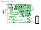
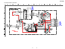
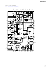
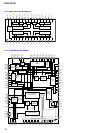
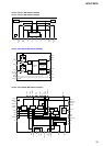
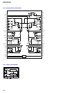
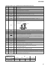
• BD (MD) BOARD IC151 CXD2662R
(DIGITAL SIGNAL PROCESSOR, DIGITAL SERVO PROCESSOR, EFM/ACIRC ENCODER/DECODER,
SHOCK PROOF MEMORY CONTROLLER, ATRAC ENCODER/DECODER)
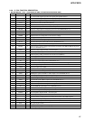
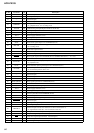
Pin No. Pin Name I/O Description
1 MNT0 (FOK) O
Focus OK signal output terminal “H” is output when focus is on (“L”: NG)
Not used (open)
2 MNT1 (SHOCK) O
Track jump detection signal output to the MD mechanism controller (IC1001)
3 MNT2 (XBUSY) O
Busy monitor signal output to the MD mechanism controller (IC1001)
4 MNT3 (SLOCK) O
Spindle servo lock status monitor signal output to the MD mechanism controller (IC1001)
5SWDTI
Writing serial data signal input from the MD mechanism controller (IC1001)
6 SCLK I (S)
Serial data transfer clock signal input from the MD mechanism controller (IC1001)
7 XLAT I (S)
Serial data latch pulse signal input from the MD mechanism controller (IC1001)
8 SRDT O (3)
Reading serial data signal output to the MD mechanism controller (IC1001)
9 SENS O (3)
Internal status (SENSE) output to the MD mechanism controller (IC1001)
10 XRST
I (S)
Reset signal input from the MD mechanism controller (IC1001) “L”: reset
11
SQSY O
Subcode Q sync (SCOR) output to the MD mechanism controller (IC1001)
“L” is output every 13.3 msec Almost all, “H” is output
12
DQSY O
Digital In U-bit CD format subcode Q sync (SCOR) output to the MD mechanism controller
(IC1001) “L” is output every 13.3 msec Almost all, “H” is output
13 RECP I
Laser power selection signal input from the MD mechanism controller (IC1001)
“L”: playback mode, “H”: recording mode
14 XINT O Interrupt status output to the MD mechanism controller (IC1001)
15 TX O
Magnetic head on/off signal output to the over write head drive (IC181)
16 OSCI I System clock signal (90.3168 MHz) input terminal
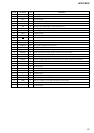
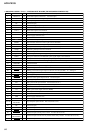
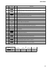
17 OSCO O System clock signal (512Fs=90.3168 MHz) output terminal Not used (open)
18 XTSL I
Input terminal for the system clock frequency setting
“L”: 45.1584 MHz, “H”: 90.3168 MHz (fixed at “H” in this set)
19 DIN0 I
Digital audio signal input terminal when recording mode Not used
20
DIN1 I Digital audio signal input terminal when recording mode
21
DOUT O Digital audio signal output terminal when playback mode
22
DADTAI I Recording data input from the A/D converter (IC1005)
23
LRCKI I
L/R sampling clock signal (44.1 kHz) input from the D/A converter (IC1006), A/D converter
(IC1005)
24
XBCKI I Bit clock signal (2.8224 MHz) input from the D/A converter (IC1006), A/D converter (IC1005)
25
ADDT I Recording data input terminal Not used (fixed at “L”)
26
DADT O Playback data output terminal Not used (open)
27
LRCK O L/R sampling clock signal (44.1 kHz) output terminal Not used (open)
28
XBCK O Bit clock signal (2.8224 MHz) output terminal Not used (open)
29 FS256 O
Clock signal (11.2896 MHz) output terminal Not used (open)
30 DVDD — Power supply terminal (+3.3V) (digital system)
31 to 34
A03 to A00 O Address signal output to the D-RAM (IC152)
35
A10 O
Address signal output to the D-RAM (IC152)
36 to 40
A04 to A08 O Address signal output to the D-RAM (IC152)
41 A11 O
Address signal output to the external D-RAM Not used (open)
42 DVSS — Ground terminal (digital system)
43 XOE O Output enable signal output to the D-RAM (IC152) “L” active
* I (S) stands for schmitt input, I (A) for analog input, O (3) for 3-state output, and O (A) for analog output in the column I/O.