


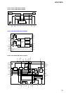
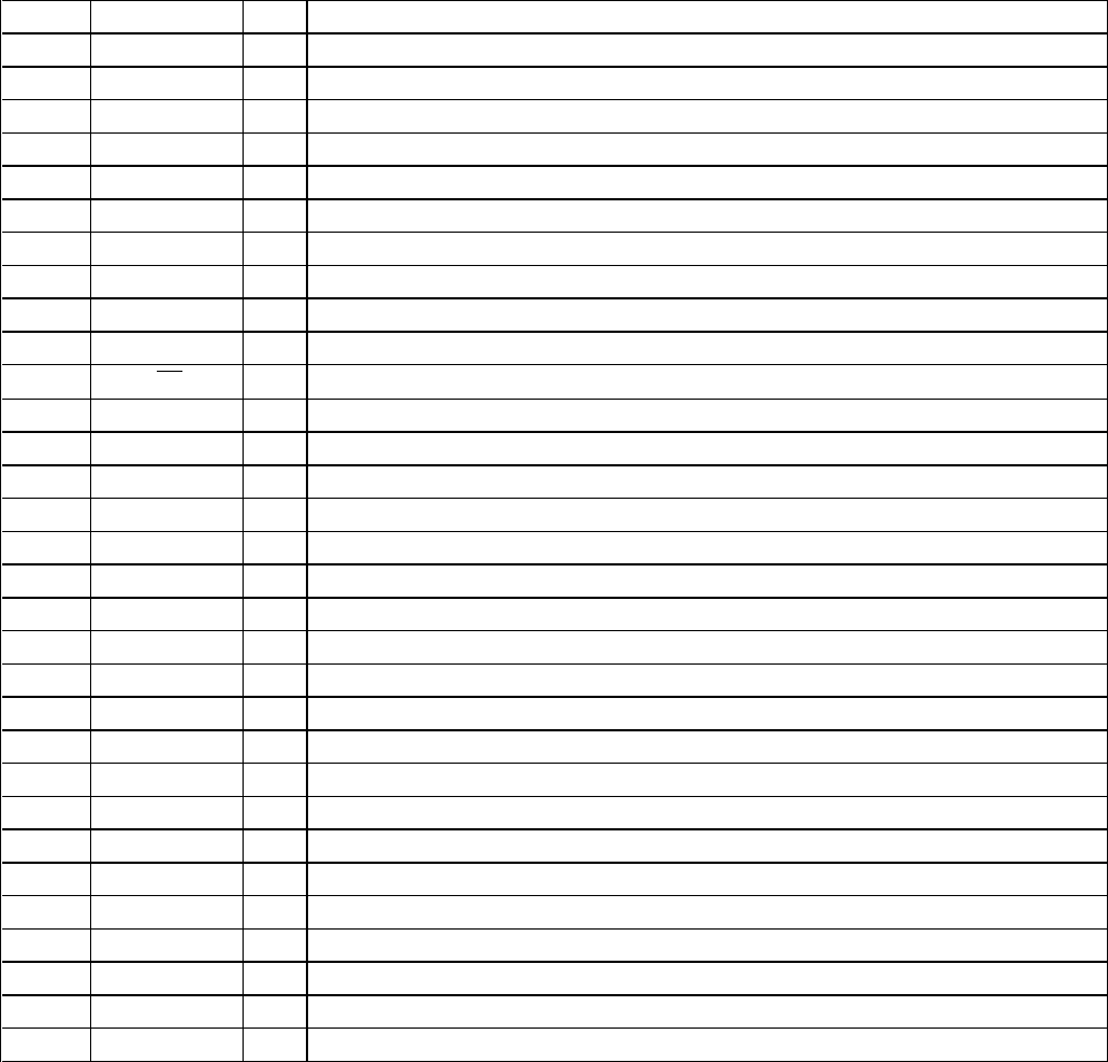
87
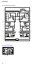
HCD-PX333
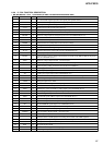
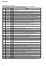
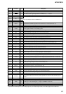
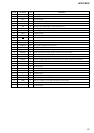
Pin No. Pin Name I/O Description
74 VCC3
— Power supply terminal (+3.3V)
75 A18 O
Address signal output Not used (open)
76 VSS3
— Ground terminal
77 to 85 A17 to A9 O
Address signal output Not used (open)
86 to 89 SEL3 to SEL0
I Model destination setting input terminal
90 WP O
Writing protect signal output Not used (fixed at “L”)
91 VCC4
— Power supply terminal (+3.3V)
92 A8 O
Address signal output Not used (open)
93 VSS4
— Ground terminal
94 to 100 A7 to A1 O
Address signal output Not used (open)
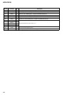
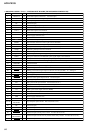
102 to 113
Two-way data bus Not used (open)
114 CLIP SEL
O Not used (open)
115
I2CBUSY
I/O
Busy signal input/output for the IIC bus
116 DALOCK
I Lock signal input from the D/A converter (IC1006)
117 LINE-MUTE O
Audio line muting on/off control signal output
118 ADPDWN
O Power down detection signal output to the A/D converter (IC1005)
119 to 12
2
D3 to D0 I/O
Two-way data bus Not used (open)
123 SPDIF-CUT O
MD/CD digital input selection signal output terminal Not used (open)
124 OPTSEL O
CD/optical digital input selection signal output to the digital signal selector (IC1008)
125 to 12
9
—
O
Not used (open)
130 VSS5
— Ground terminal
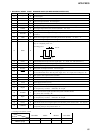
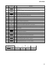
131
—
O
Not used (open)
132 VCC5
— Power supply terminal (+3.3V)
133 OP-LEVEL
I Optical pick-up voltage input from the automatic power control circuit
134 to 13
9
—
O
Not used (open)
140 AVSS
— Ground terminal (for analog system )
141
—
O
Not used (open)
142 VREF I Reference voltage (+3.3V) input terminal (for A/D converter)
143 AVCC
— Power supply terminal (+3.3V) (for analog system )
144
—
O
Not used (open)
LB
D15 to D4 I/O
Not used (open)O
101