


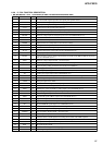

86
HCD-PX333
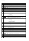
Pin No. Pin Name I/O Description
31 C2-PWM-B
O Not used (open)
32 XINT
I Interrupt status input from the CXD2662R (IC151)
33
— O Not used (open)
34 XELT
I Not used (open)
35 WR-PWR
O
Laser power select signal output to the CXD2662R (IC151) and HF module switch circuit
“L”: playback mode, “H”: recording mode
36 I2CCLK
I/O Shift clock signal input/output terminal for the IIC bus
37 I2CDAT I/O
Data input/output terminal for the IIC bus
38 SWDT O
Writing data output to the CXD2662R (IC151)
39 VCC1
— Power supply terminal (+3.3V)
40 SRDT I
Reading data input from the CXD2662R (IC151)
41 VSS1
— Ground terminal
42 SCLK O
Serial clock signal output to the CXD2662R (IC151)
43 REC-SW I
Detection input from the recording position of over write head (HR901) detect switch (S105)
“L” recording mode
44 CLIPDTO
O Serial data output terminal
45 CLIPDTI
I Serial data input terminal
46 CLIPCK
O Serial clock signal output terminal Not used (open)
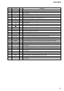
47 DIG-RST O
Reset signal output to the CXD2662R (IC151) and BH6519FS (IC141) “L”: reset
48 SENS
I Internal status (SENSE) input from the CXD2662R (IC151)
49 PLAY-SW I
Detection input from the playback position of slider (eject) detect switch (S104)
“L” playback mode
50 XLAT
O Serial data latch pulse signal output to the CXD2662R (IC151)
51 OUT-SW I
Detection input from the loading-out detect switch (S103)
“L” at a load-out position, others: “H”
52
—
I
Not used (open)
53
— O Not used (open)
54
—
I
Not used (open)
55
— O Not used (open)
56 MNT2 (XBUSY) I
Busy signal input from the CXD2662R (IC151)
57 VSS2
— Ground terminal
58 MNT1 (SHOCK) I
Track jump detection signal input from the CXD2662R (IC151)
59 VCC2
— Power supply terminal (+3.3V)
60 EEP-WP O
Writing protect signal output to the EEPROM (IC195)
61 SDA I/O
Two-way data bus with the EEPROM (IC195)
62
BCLK/ALE/CLKO
O Not used (open)
63 OE O
Data reading strobe signal output Not used (open)
64
BHE/CASH O Not used (open)
65 WE O
Writing enable signal output Not used (open)
66 SCL O
Clock signal output to the EEPROM (IC195)
67 REFLECT I
Detection input from the disc reflection rate detect switch (S102-1)
“L”: high reflection rate disc, “H”: low reflection rate disc
68 PROTECT I
REC-proof claw detect input from the protect detect switch (S102-2) “H”: write protect
69 CS0 O
Chip select signal output Not used (open)
70 CS1 O
Chip select signal output terminal Not used (open)
71. 72
——Not used (open)
73 A19 O
Address signal output Not used (open)