


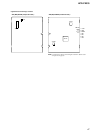


5555
HCD-PX333
C
B
These are omitted.
E
Q
B
These are omitted.
CE
Q
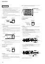
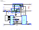
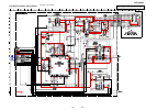
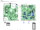
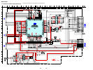
Note on Printed Wiring Boards:
• X : parts extracted from the component side.
• Y : parts extracted from the conductor side.
• b : Pattern from the side which enables seeing.
(The other layers' patterns are not indicated.)
Caution:
Pattern face side: Parts on the pattern face side seen from
(Side A) the pattern face are indicated.
Parts face side: Parts on the parts face side seen from
(Side B) the parts face are indicated.
• Indication of transistor.
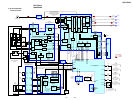
Note on Schematic Diagram:
• All capacitors are in µF unless otherwise noted. pF: µµF
50 WV or less are not indicated except for electrolytics
and tantalums.
• All resistors are in Ω and
1
/
4
W or less unless otherwise
specified.
• % : indicates tolerance.
•
f
: internal component.
• 5 : fusible resistor.
• C : panel designation.
• A : B+ Line.
• B : B– Line.
• Voltages are taken with a VOM (Input impedance 10 MΩ).
Voltage variations may be noted due to normal produc-
tion tolerances.
• Waveforms are taken with a oscilloscope.
Voltage variations may be noted due to normal produc-
tion tolerances.
• Circled numbers refer to waveforms.
• Signal path.
F : FM
J : CD PLAY
E : MD PLAY
j : MD REC
q : DIGITAL OPTICAL IN
d : TAPE IN (PLAY)
G : TAPE OUT (REC)
• Abbreviation
MY : Malaysia model
SP : Singapore model
HK : Hong Kong model
AUS : Australian model
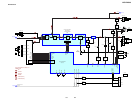
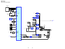
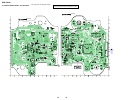
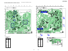
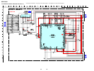
• Circuit Boards Location
The components identified by mark 0 or dotted
line with mark 0 are critical for safety.
Replace only with part number specified.
6-2. NOTE FOR PRINTED WIRING BOARDS AND SCHEMATIC DIAGRAMS
(In addition to this, the necessary note is printed in each block)
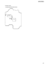
PANEL board
JACK board
VOL board
BL board
REC board
POWER board
AMP board
SP board
TUNER PACK
MAIN board
BD(MD) board
LOADING board
MD DIGITAL board
BD(CD) board